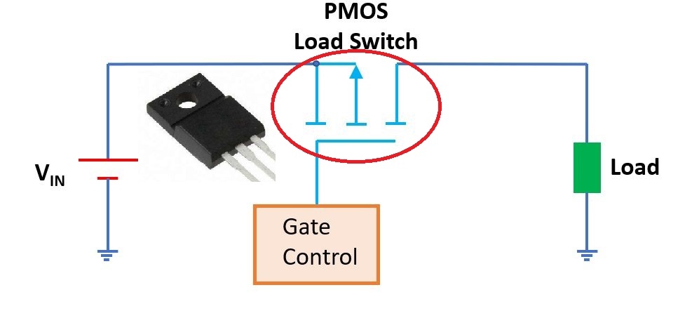
Today, as many electronic devices are becoming mobile and portable, low power consumption is one of the most important requirements. We need carefully select the circuits and components for efficient power management to extend the battery life. In many electronic devices, the loads normally are not always on or off, but working based on a pattern, or duty cycle. A temperature may only need to sample the environment once every minute, while the RF module only needs to turn on when the data is ready for transmission. Therefore, we may want to turn the power off to these modules when they really don’t need the power at the moment and then turn them on when they need. This is when the load switches are used based on the designated duty cycles of their applications. The load switches have been widely used in laptops, smart phones, IoT (Internet of Things) devices and hand-held portable device. The basic form of a load switch is shown below:
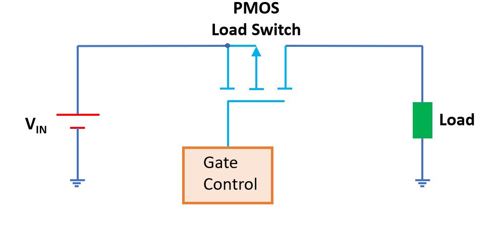
As shown in the above figure, the load switch is placed in between of the power source and the load. The load switch is controlled by the microcontroller that decides when to turn on/off the load switch to connect or disconnect the load to the power rail. The core of a load switch is the pass transistor that is often a MOSFET to pass the power supply to the load to be controlled.
How to select the load switch to be used in a specific application is determined by many factors, including the cost, form factor, functionality and availability. All of these factors may change from application to application. Therefore, we cannot rely o them to give a common guidelines on how to select the load switches. If we decide the selection based on the functionalities of the load switch, then we can make the good selections applicable to all scenarios.
The load switch is used to turn on/off the loads. Therefore, its performance is determined by the two distinct periods, the ON time and OFF time. When the load switch is turned off, the key parameter to affect the system is the quiescent current that contributes to the standby power consumption and the turn-off characteristics.
When the load switch is on, it becomes part of the load of the power supply. Therefore, its own characteristics can affect the overall performance of the system, which includes the ON resistance, control topology, gate-to-source voltage, inrush current and turn on speed, etc.
ON resistance RDS(on)
The on resistance of a MOSFET is the resistance of the channel between the drain and source of the MOSFET when it is in conducting operation. The higher the on resistance, the more power loss it causes. According to semiconductor physics, the on resistance of MOSFETs is decided by the dimensions of the device channel and the type of the material forming the channel. Traditionally, P-channel MOSFET cannot reach the same RDS(on) performance of an N-channel MOSFET with the same die size. The majority carriers in an N-channel MOSFET are electrons, whose mobility is approximately 2 to 3 times higher than that of a P-channel. To achieve the same level of RDS(on), the P-channel die must be made 2 to 3 times larger than the N-channel. With the larger die size, we can gain the advantages of lower thermal resistance and higher current rating for the P-channel MOSFET, but lose dynamic performance due to the larger gate capacitance. Generally, we make selections between the P-channel and N-channel based on the specific requirements of applications.
Low-frequency applications
For low-frequency applications, the conduction loss caused by the load switch is the primary concern. Therefore, RDS(on) is the only requirement matters the performance. So we can select P-channel MOSFET over N-channel MOSFET. The P-channel MOSFET will have larger chip size to provide a low RDS(on). Since the working frequency is low, e.g., from 10 to 50k Hz, the loss in dynamic performance due to the dimensions of device structure is not significant. On the other side, we gain advantages of better thermal performance and higher current rating.
High-frequency applications
For high-frequency applications, e.g., high frequency PWM, the dominant loss is caused by the switching operation. An N-channel MOSFET with the same chip size as a P-channel MOSFET has comparable dynamic and thermal performance due to the similar gate charges and structural dimensions, but the P-channel MOSFET has a larger RDS(on) due to the much lower mobility rate. Selecting between the P-channel and N-channel MOSFET is totally based on the RDS(on) and gate charge QG.
Mobile applications
Other than the distinct separation between the low- and high- frequency applications, we have the popular mobile applications, which have strict requirements for the size. Normally, such applications demand a power less than 10W. For such applications, the design goal is to achieve high efficiency while keeping the size acceptable according to the designs. Fast switching frequencies can help reduce the size of the inductors. Moreover, we can use the P-channel MOSFET that eliminates the need for extra gate driver circuitry to further save space.
Gate-to-source voltage, VGS
As we have mentioned, the on resistance RDS(on) between the drain and source is one of the most important characteristics of the MOSFET. The gate-to-source voltage determines the RDS(on). The MOSFET turns on when the applied gate-to-source voltage is higher than the threshold voltage, Vth.
According to theory of MOSFET, the relationship between the on resistance RDS(on) and the gate-to-source voltage VGS is
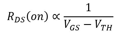
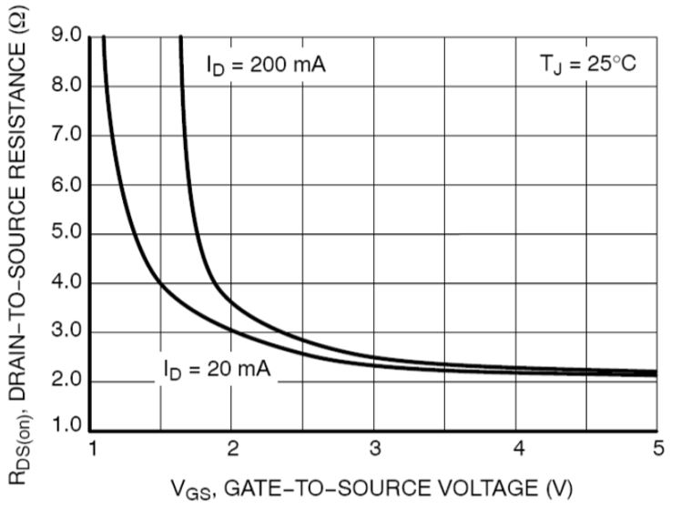
We know the MOSFET’s “on state” consists of a triode region and saturation region. The triode region is where the above formula refers to and the resistance in the triode region is extremely high. Therefore, the desirable RDS(on) is the value falling in the saturation region as shown in the above plot where the RDS(on) begins to flatten out.
Turn on characteristics
When the load switch is turned on, its dynamic characteristics affect the overall performance of the system, such as the inrush current and turn-on speed. The inrush current is caused by the capacitive loading characteristics of the load when the power is applied to it. The capacitive load starts to charge and it appears to have no resistance. The result is a huge current spike and corresponding voltage sag on the power supply output. The slew rate of the voltage being applied to the input capacitance and the capacitance itself determines the inrush current:
IINRUSH = CL x (dv/dt), where CL is the input capacitance and dv/dt is the slew rate of input voltage. As an example, for a 20 uF input capacitor, if the slew rate of the voltage is 4 V/µs, then the inrush current is 20 x (4) = 80 A. If the power supply, e.g., the battery, has an ESR (equivalent series resistance) of 0.02 Ω, the voltage sag on the battery will be 0.02 x 80 = 1.6 V.
This figure shows the effect of inrush current caused by a 100µF load capacitance. Without any slew rate control, the inrush current peaks at about 6.88A and forces the voltage rail to drop from 3.3V down to 960mV. (By Texas Instruments)
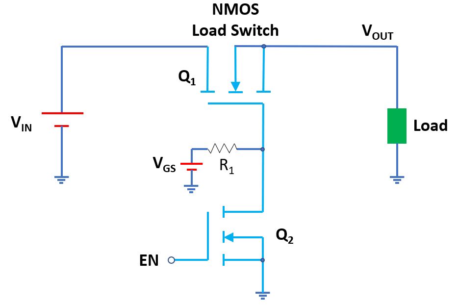
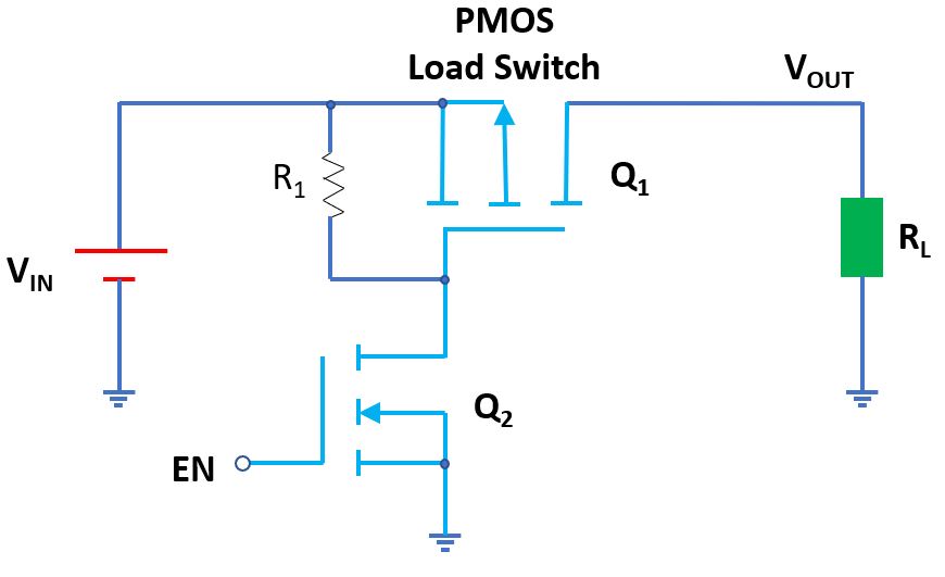
The effect of the inrush current can be mitigated by specifying a settling time during which the system is kept in a reset state until the voltage stabilizes. Different load switches have different methods for reducing the slew rate. The following circuit uses an external resistor R1 an capacitor C1 to reduce the turn on speed of the pass transistor.
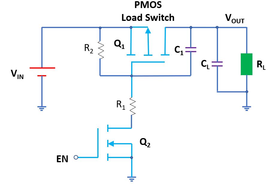
In the circuit, the R1 and R2 form a voltage divider to determine the gate voltage and they can be determined by using the following equation:
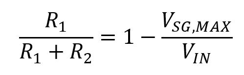
VSG,MAX can be found in the datasheet. To calculate R1, we can use a value between 1k and 10kΩ for R2. The C1 combining with R1 determines the turn-on speed of the pass transistor and it can be calculated. The selection of R1, R2 and C1 is critical to the performance of the load switch. C1 must be much larger than the gate capacitance of the pass transistor to be able to control the slew rate.
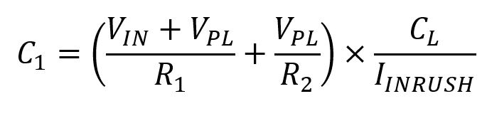
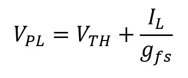
Where the plateau voltage VPL is defined as:
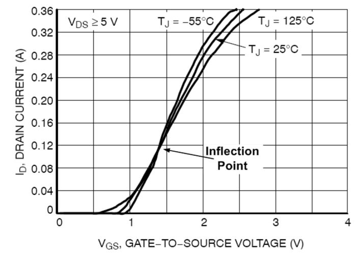
As important as the inrush current to the performance of load switches, the turn-on speed is one of the key parameters to be considered in selection of the right load switch for your applications. Fast turn-on speed can cause inrush current. A slower turn-on speed is helpful for reducing the input current spikes but may cause other problems. As shown in the above figure, MOSFETS operates at different temperatures show different characteristics but all the transfer curves for different temperatures will intersect at a specific VGS, which is called the inflection point. Above the inflection point, RDS(on) increases as temperature increases, so the current decreases. For parallel power distribution, the current decreases in one branch will cause the current increases in less resistive branch. Therefore, the final result is a balanced current distribution among all the loads. Below the inflection point, the MOSFET behaves as a BJT (Bipolar Junction Transistor) that conducts higher current as it’s heated up and the current continuously increases as temperature rises. This is the situation normally leads to the thermal runaway of the device. The selection of the appropriate gate-to-source voltage is very important to keep the load switch from thermal runaway.
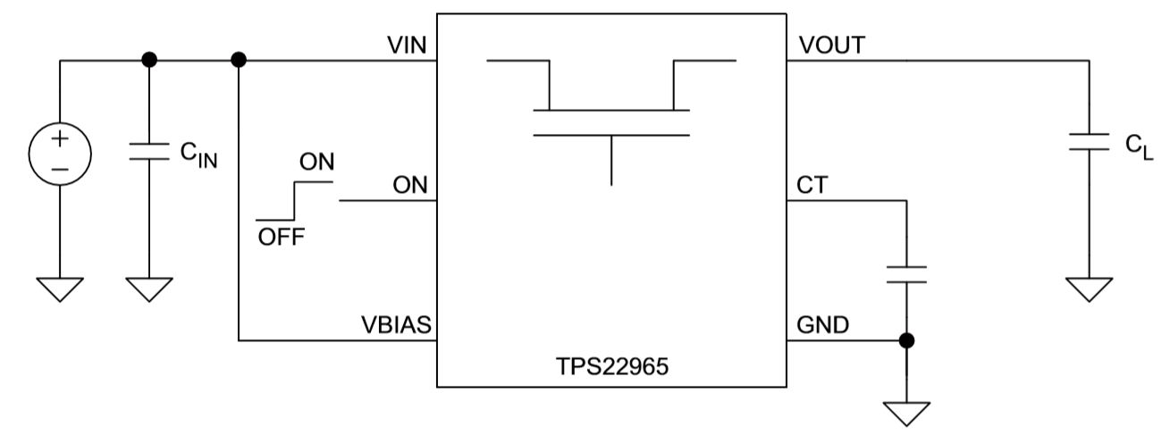
Texas Instruments load switches feature a controlled rise time, and for some products, the rise time can be adjusted. The rise time of the load switches can be increased by adding an external capacitor between the CT pin and GND pin as shown below in the application circuit of TPS22965.
The following two figures show the different rising times of TPS22965 load switch for different CT capacitance used for a 22 µF capacitive load.
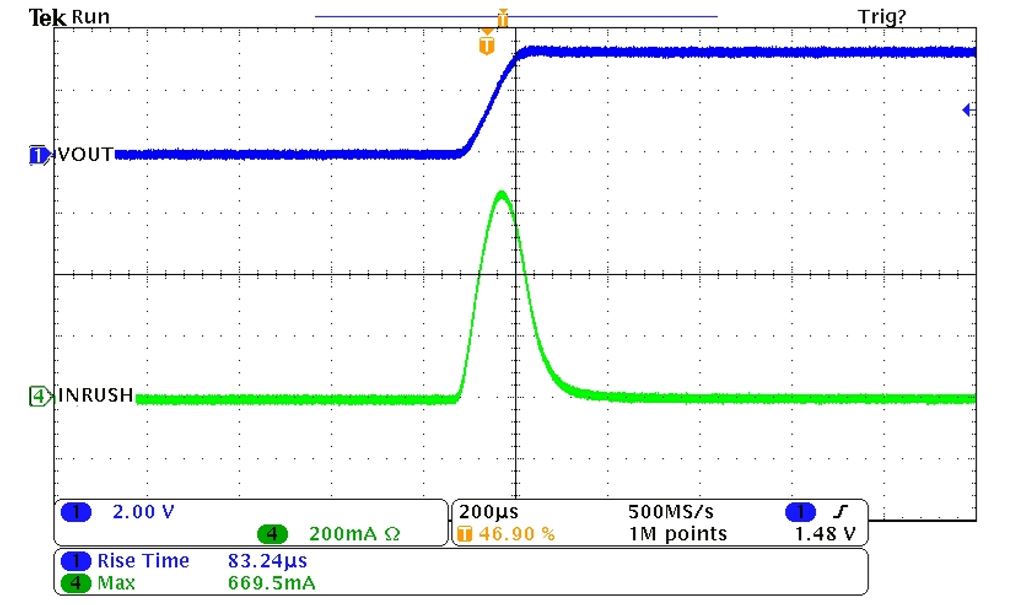
This figure shows the rise time and the inrush current of the load switch when there is no additional capacitance is added to the CT pin of TPS22965. The rise time is so short that it may not be sufficient to limit the inrush current to the desired peak value. The figure indicates the rise time is about 120µs and the peak current is above 650mA.
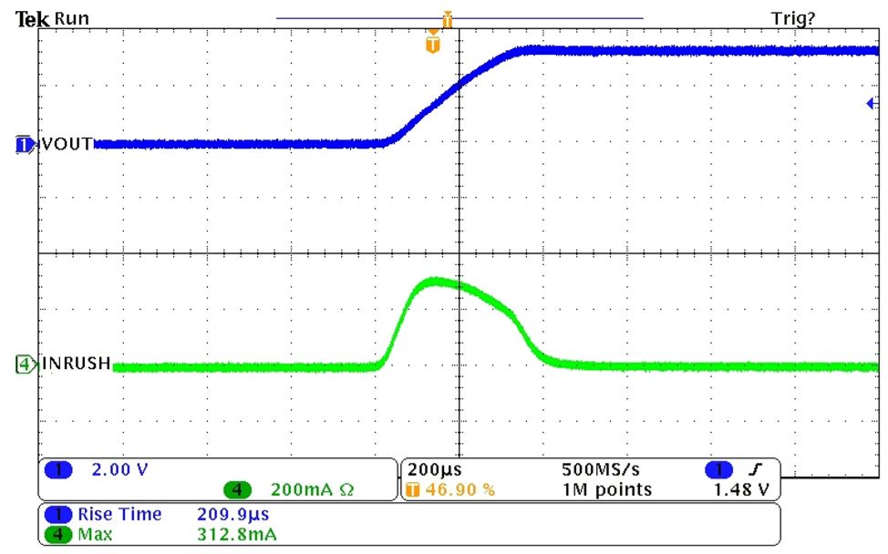
This figure shows the rise time and the inrush current of the load switch when there is an additional 150pF capacitance is added to the CT pin of TPS22965. The rise time is so short that it may not be sufficient to limit the inrush current to the desired peak value. The figure indicates the rise time is extended to about 320us and the peak current is reduced to just about 360mA.