Skip to content
OnElectronTech

OnElectronTech

Electronics for a better life!

  • Home
  • Blog
  • About Us
  • Login
Main Menu

EMI

Electronics / EMC / EMI / PCB / RFI

PCB Layout Design Tips – Grounding Considerations

December 16, 2018January 25, 2019 - by electron_one - Leave a Comment

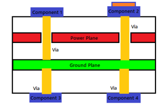
PCB layout designers have always been concerned about these prominent questions, as how to plan an effective grounding system on the board, whether to route all grounds like analog, digital …

PCB Layout Design Tips – Grounding Considerations Read More

Latest Posts

Estimation of SOH (State of Health) of Li-ion Batteries Using Incremental Capacity Analysis (ICA)

February 27, 2023

Impact of AI (Artificial Intelligence) and energy storage on renewable energy trends in 2023

January 31, 2023January 31, 2023

Solar-Wind Hybrid Energy Harvesting Systems Offering High Efficiency and More Advantages

December 31, 2022

PV-TE (Photovoltaic-Thermoelectric) Hybrid Energy System – Concepts and Performance

December 30, 2022

PCMs (Phase Change Materials) are Efficient Storage for Renewable Energy Sources

December 24, 2022

Categories

Tags

ADAS (4) Battery (11) Communication (10) Components (4) Conference (44) Consumer Electronics (10) Electronics (22) Energy harvesting (4) Experiment (6) GaN (4) Hall Effect Sensor (3) IMU (5) Internet of Things (13) IoT (13) Lab (7) LDO (7) LED (8) LIDAR (5) Load Switch (10) Medical (3) MEMS (6) MOSFET (7) Nanomaterials (14) New product (55) New tech (22) Optics (4) Passive Component (6) PCB (3) Photodiode (2) Physics (11) PMIC (11) Power (44) Power Electronics (24) Power Switch (12) Renewable (11) RF (4) Self-driving (3) Semiconductor (27) Sensor (40) Tech show (20) Tech Talk (29) ToF (4) USB-C (3) USB-PD (3) Wireless Sensor Network (8)

Archives

Copyright © 2023 OnElectronTech.
Powered by WordPress and HitMag.
Back to Top
  • Home
  • Blog
  • About Us
  • My Account
  • Contact Us
  • Privacy Policy
2023