Decoupling capacitor can bypass noise
Decoupling capacitors are used in circuits for primarily minimizing the effect of power supply fluctuations which can be of any frequencies. These anomalies of various frequencies behave differently. But all these are considered as noises and impose adverse effects to the circuit that induce them. For instance, an instantaneous dip will be resulted in power rail voltage in reaction to a sudden turning on or off a large load, or, the ringing effect of the output voltage of a switching mode power supply (SMPS), or the low frequency ripples in the output voltage of a full bridge rectifier, etc. As we have learned from electrical engineering courses that capacitors block DC or show resistance to low-frequency signals but allow high-frequency signals to pass. This unique characteristic of capacitors makes them ideal for bypassing high-frequency noise to the ground to improve the input of the circuit and avoid further spreading the high-frequency noise to other parts of the system. In SMPS, even though many design techniques have been used to mitigate the unwanted high dv/dt and di/dt irregularities in their outputs, stray high-frequency components can be still propagating to the power rail. Therefore, bypass capacitors are needed as the last fence to the noise for sensitive IC components.
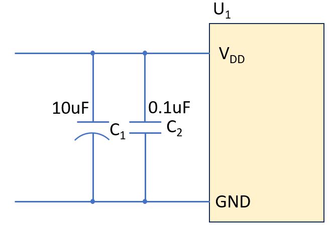
The lower value capacitor (0.1uF capacitor) in the above circuit is responsible for high-frequency noise filtering. We should select a low value (typically from 0.01uF to 0.1uF) SMD (surface mounted device) ceramic capacitor. When design PCB, the decoupling capacitor used for bypassing noise should be placed as close as possible to the VDD pin of the IC via short traces and vias to the nearest ground plane to reduce series inductance. The ceramic capacitor selected should have low inductance.
Decoupling capacitors can stable voltage
The power supplies for IC are not always as stable as a straight line. But as far as the specs in the datasheet permits, we live with the small variations of power supply output. Some circuits can tolerate lots of fluctuations, but some cannot. As a rule of thumb, we want the power supplies to provide stable rail voltage as much as possible. The decoupling capacitors can be used to act against instantaneous voltage fluctuations in voltage for a specific IC component. In this case, the decoupling capacitor behaves like a reservoir for storing electric energy and compensates sudden voltage drop to keep the supply voltage stable. The purpose of this capacitor is to temporarily decouple the IC component from the power supply to mitigate the undesirable voltage changes in the power supply.
In ADC (Analog-to-Digital Converter) circuits, an accurate reference voltage is critical for good results. In an ideal ADC circuit without conversion errors or gain errors, the digital output of ADC can be simply written as
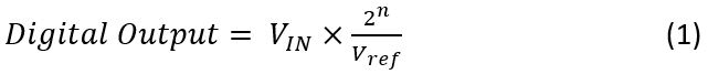
The digital output is directly related to the reference voltage. Therefore, we must stabilize the reference voltage.
In some other applications, even the voltage fluctuations are still contained within the specs, the overall performance is still degraded. For example, we have an op amp circuit show below.
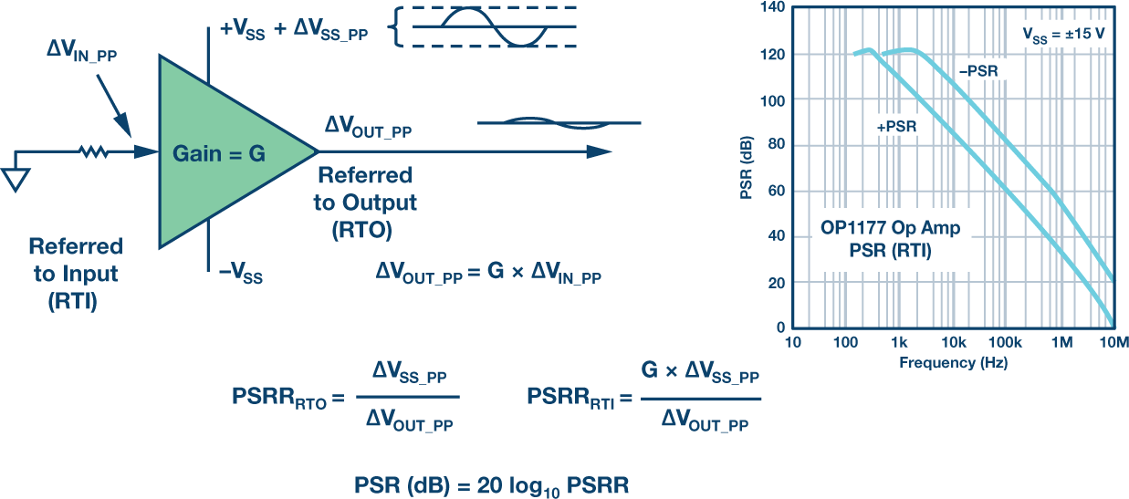
The PSRR (Power Supply Rejection Ratio) defines how sensitive an amplifier is to the power supply voltage changes. The PSR curves on the left in the above figure shows both the positive and negative PSRR curves decrease greatly in higher frequency domain where the noise on the power rails couples to the output.
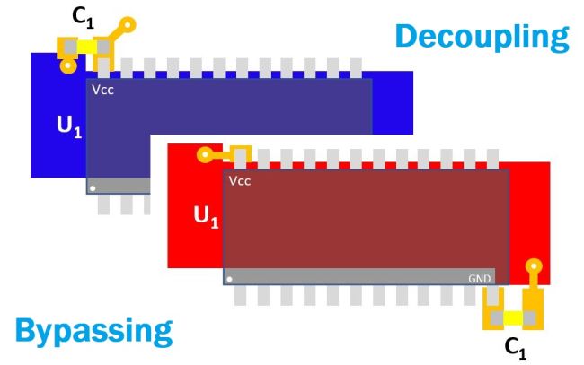
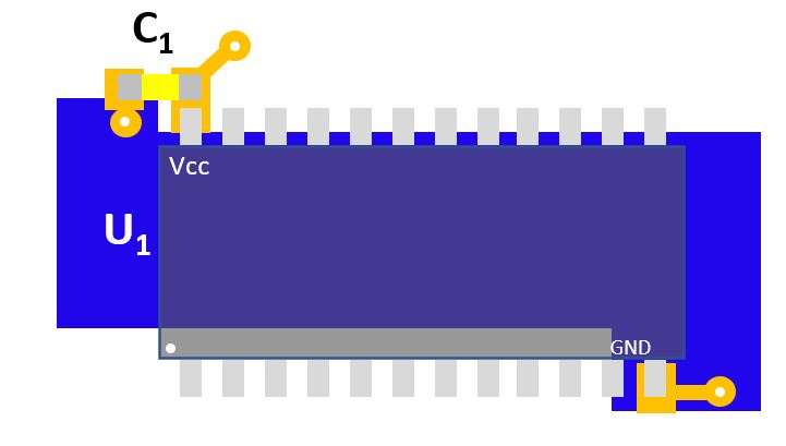
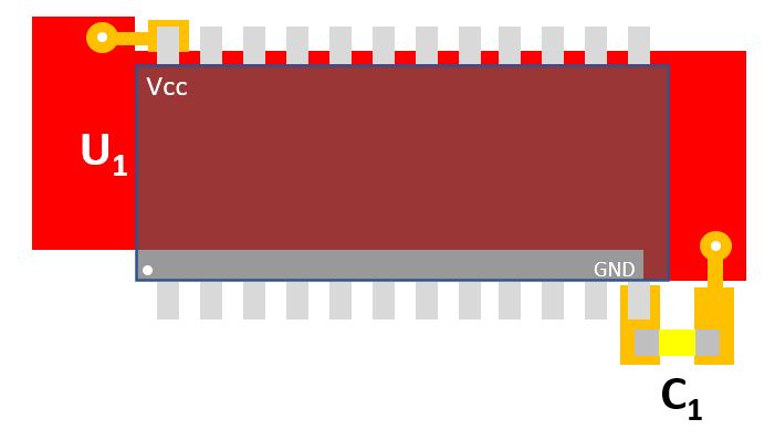
Decoupling capacitor placement on PCB
The decoupling capacitors must be placed as close as possible to the power supply in or ground pin of the IC component using short trace and vias to minimize the undesirable inductance and impedance in the ground connection. The following figures show the two options for placing the decoupling capacitor, on the power supply pin or on the ground pin.
Reference
https://www.analog.com/en/analog-dialogue/studentzone/studentzone-april-2017.html
https://www.onelectrontech.com/pcb-layout-guidelines-for-decoupling-and-bypassing-capacitors/