
Since University of Manchester scientists Andre Geim and Konstantin Novoselov won 2010 Nobel Prize in Physics for their groundbreaking experiments for fabricating a new magic material called graphene from natural graphite, Graphene has attracted extensive studies cross the whole world for broad-reaching applications in optics, electrical, mechanical, nano fabrication, energy, biomedical, and medicine, etc.
Graphene, a perfect atomic lattice of one carbon atom thick shows extraordinary characteristics explainable only by quantum physics. Its remarkable properties come from the magic atomic scale hexagonal “honeycomb” as shown in the following figure.
Graphene’s nanostructure is created by the same bonding mechanism seen in carbon nanotubes and polycyclic aromatic hydrocarbons. Every carbon atom in the graphene 2D sheet is bonded to three carbon atoms by a σ-bond (sigma bond) due to the sp2 hybridization between the s and 2 p orbitals. The sigma bond is a strongest covalent chemical bond, which attributes to its excellent physical and chemical characteristics. In each sigma band, the center carbon atom uses three of its valence electrons and contributes one extra p orbital electron to a valence band. Because of Pauli principle, the sigma bands have a filled shell thus form a deep valence band that extends over the whole graphene sheet. Electronically, graphene as a semiconductor demonstrates also properties of semimetal with zero-band-gap due to its valence band touched by the conduction band only at six points (Dirac Points). The extraordinary electronic properties of graphene can be explained by the theories of massless relativistic electrons that show linear energy – momentum relationship. This phenomenon provides insight into making new electronic devices, such as high-frequency field-effect transistors with bipolar conduction and ultrafast photodetectors, etc.
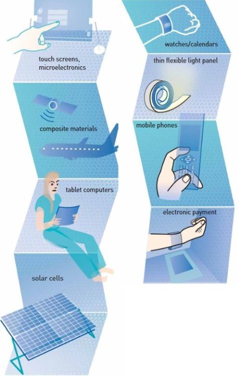
Since the discovery of graphene, many fabrication methods have been invented, such as micromechanical exfoliation (as that for winning Nobel Prize by Geim and Novoselov), Liqud-phase exfoliation (LPE), Chemical Vapor deposition (CVD), Flame synthesis and pulsed laser deposition (PLD), etc. Now, it’s time to use graphene materials in desirable applications.
Next-generation super computers
Graphene has the highest conductivity for high-frequency circuits that is the required components for making high speed super computers that requires high speed and low energy consumption.
Space elevator cables
In scientific fictions, long cables tying the satellites to the ground for energy and information transmission are becoming reality because of the extraordinary mechanical and electrical properties, such as high tensile strength and high conductivity that graphene has shown.
Materials for making LCD
Graphene is an optically transparent material due to its thin layer structure. It’s found that the optic opacity is linearly related to the number of the stack layers. For example, one layer graphene only absorbs 2.3% of light. So a 10 layers of graphene may absorb up to 23% and let 77% of light to pass through. The unique optical properties of graphene can be used for making new generations of LCD devices.
New solar cell materials
Graphene is transparent and can be used to make a conductive film that is literally fully transparent to all infrared bands including middle to far end infrared bands, which is an advantage over the traditional solar sell material, silicon, which cannot absorb infrared light. Additionally, graphene has higher efficiency in converting sunlight to electricity in that a single photon absorption by graphene can generate multiple electron-hole pairs in comparison to silicon that only generates one electron out of one photon.
Solar thermal energy harvesting
Structured Graphene Metamaterial (SGM) has excellent thermal conductivity due to its ultrathin structure. With flexible wavelength tunability, omnidirectional absorption, excellent photothermal performance and high thermal stability, SGM shows higher than 90% solar-to-thermal conversion efficiency and 96% of solar-to-vapor conversion efficiency, which make the SGM an excellent solar thermal absorber for energy harvesting.
Photodetector sensors
Graphene is highly transparent due to its thin atomic structure. This is as a drawback for light detection by graphene alone. But graphene coupled with strong light-absorbing materials can be an excellent candidate as photodetectors due to the frequency-dependent photon absorption and very high carrier mobility in graphene. Graphene quantum dots made of this compound can be used to fabricate high performance photodetectors as broadband image sensors in CMOS cameras.


Reference
https://nanografi.com/blog/60-uses-and-applications-of-graphene-nanografi-/
https://www.nobelprize.org/prizes/physics/2010/press-release/
It’s still all about graphene. Nature Mater 10, 1 (2011). https://doi.org/10.1038/nmat2938
Geim, A., Novoselov, K. The rise of graphene. Nature Mater 6, 183–191 (2007). https://doi.org/10.1038/nmat1849
https://www.mub.eps.manchester.ac.uk/graphene/2020/12/the-accidental-nobel-laureates-10-years-on/
Carvalho, A. F., Kulyk, B., Fernandes, A. J., Fortunato, E., & Costa, F. M. (2022). A review on the applications of graphene in mechanical transduction. Advanced Materials, 34(8), 2101326.
Han, T. H., Kim, H., Kwon, S. J., & Lee, T. W. (2017). Graphene-based flexible electronic devices. Materials Science and Engineering: R: Reports, 118, 1-43.
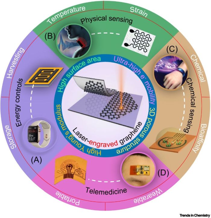
Wang, M., Yang, Y., & Gao, W. (2021). Laser-engraved graphene for flexible and wearable electronics. Trends in Chemistry, 3(11), 969-981.
Wang, H., Zhao, Z., Liu, P. et al. A soft and stretchable electronics using laser-induced graphene on polyimide/PDMS composite substrate. npj Flex Electron 6, 26 (2022). https://doi.org/10.1038/s41528-022-00161-z
Saraswat, V., Jacobberger, R. M., & Arnold, M. S. (2021). Materials science challenges to graphene nanoribbon electronics. ACS nano, 15(3), 3674-3708.