Analog and digital ICs on a PCB are powered by voltage regulators or various types of converters via PDNs (Power Distribution Networks). To maintain acceptable performance of the analog and digital ICs, the supplied voltages to these ICs must be within their respective requirements specified in the datasheets, like the recommended operating ranges and absolute maximum operating ranges. Therefore, the designers must carefully understand the requirements and follow strictly the requirements to ensure the circuit will not be damaged under all circumstances. Besides the conditions for device safety, there are also design margins for performance considerations. An outstanding aspect of design margins is the voltage variations of the power supplies. Small variations of the output voltages of the power supplies can cause significant performance degradation. The supply voltage fluctuation can be caused by noise, such as interference or ground loops and voltage ripples. Ideally, we expect there is no changes in the output of an amplifier exposed to small fluctuations. PSRR (Power Supply Rejection Ratio), the capability of an amplifier to maintain its output when the power supply voltage is changed is used to measure the sensitivity of the amplifier subject to the power supply variations. Basically, any noise showing up in the input supply will also propagate to the output. The following figure shows the concept of PSRR.
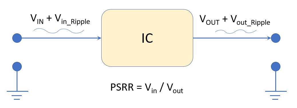
PSRR is normally defined over a very large range of frequencies, e.g., from 10 Hz to 1MHz), so logarithm is used:
PSRR = -20Log (Ripple Input)/(Ripple Output)
Where, the Ripple Input and Ripple Output are the RMS values of the input/output voltage changes. These ripples can be resulted from the AC input supply ripples at 50/60 Hz, or switching ripples from a DC-DC converter, or ripples caused by the PDN (Power Distribution Network) shared by various circuits on the same PCB. We notice the negative sign in the above equation, but normally we don’t mention the sign. Also, as shown by the above formula, PSRR is dimensionless without a unit, but we usually mention it with a unit of dB (Decibels) because of PSR (Power Supply Rejection). PSR and PSRR are usually interchangeably used without any standard limitation.
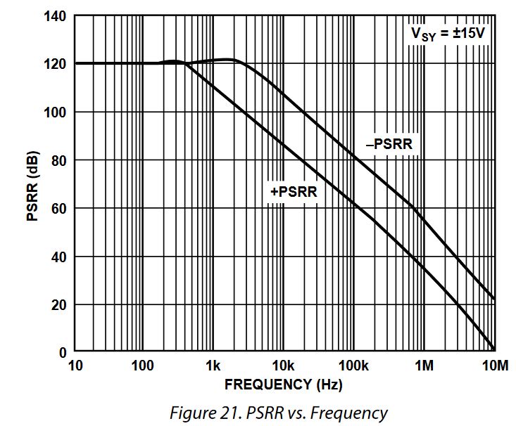
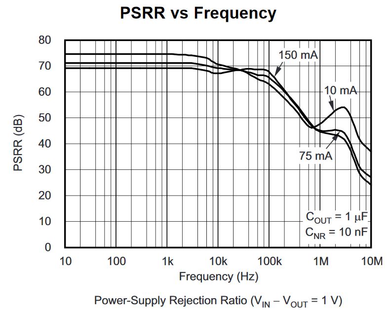
Examples of PSRR:
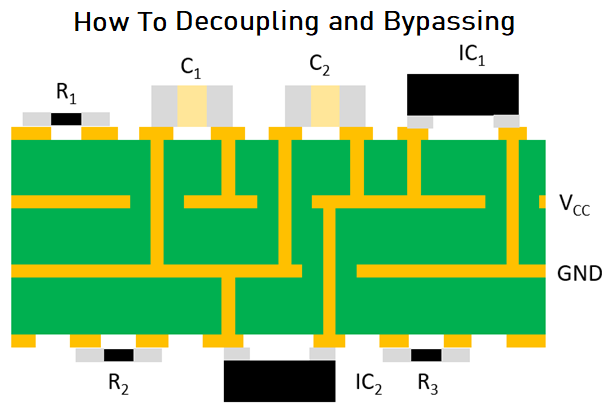
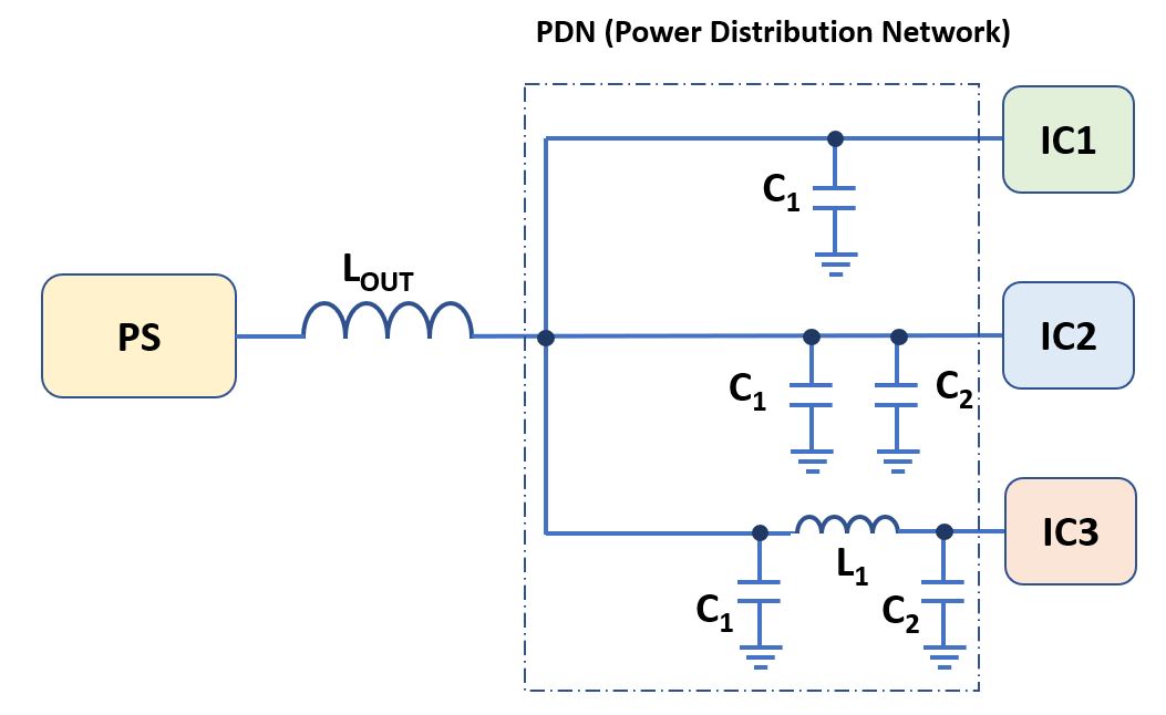
In PCB designs, we see the common use of capacitors that are placed close to the power pins of analog and digital ICs to address the degradation of PSRR. These capacitors are referred to decoupling and bypassing capacitors. Sometimes, the two terms are used interchangeably, but they demand special attention to the differences between them. By definition, decoupling capacitor functions as the isolation between two different circuits sharing the same PDN or between a local circuit from the external ones. While bypassing capacitors are used to eliminate the high frequency noise entering the circuit by bypassing it to the ground. The decoupling and bypassing capacitors can be used in stand-alone fashion or together in the parallel topology, or even in the composite connection (π structure) the power input stage as shown in the diagram below. The decoupling capacitors can not only shunt the noise to ground by also smooth out the voltage ripples. They are used to suppress the noise generated by or entering an IC, provide transient current associated with IC operations and maintaining voltage and become a part of signal path. Simply put, the purpose of a decoupling capacitor is to eliminate the power supply distortion and noise associated with the PDN and provide the power receiving device with quality DC supply.
Topologies of decoupling circuits:
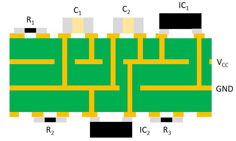
In a four-layer PCB, the top and bottom layers are component/signal layers, and the inner layers are the power and ground plane layers. AS shown in the below diagram, lots of vias are used to directly connect the power and ground pins of the ICs to the power and ground planes of the PCB to minimize the unwanted impedance in the power interconnections.
PCB layout for decoupling capacitors:
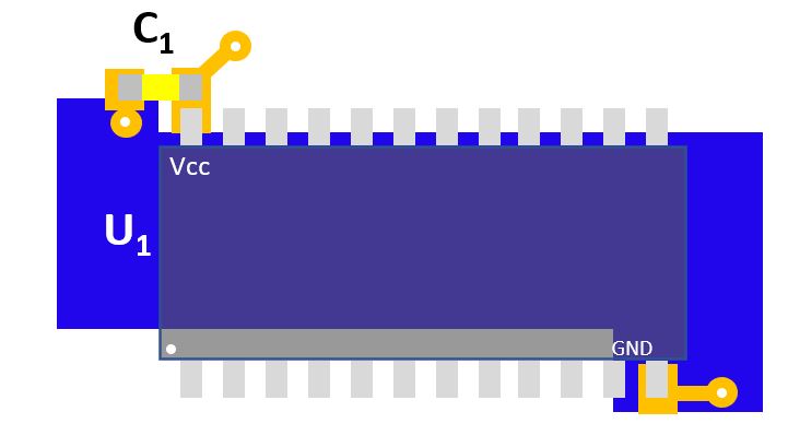
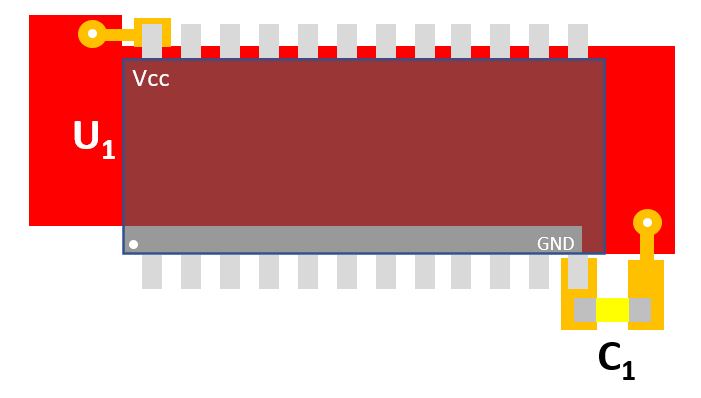
The following diagram shows a simplified circuit model of the PCB stack of the power supply, IC and ground. PCB traces have impedance due to the finite dimensions, and it causes the voltage drop between the power rail and the power pin of the receiving ICs. The decoupling capacitor is used to directly connect the local power supply VCC to the ground. To minimize the ground impedance, the decoupling capacitor must be placed as close as possible to the IC power pin. When power fluctuation occurs, the decoupling capacitor stores the energy carried along with the transient current and shunts it directly to the ground, thus maintain a relatively constant voltage at the power pin of the device. Because the ground is made as short as possible, the negligible ground impedance will not develop a significant noise voltage by the returning current. For the decoupling capacitors that are used to compensate the power supply variations at high frequencies, they must have low inductance in such frequency range and typically in the range from 0.01 uF to 0.1 uF, therefore, they are usually ceramic types. For decoupling capacitors that are used to compensate low frequency noise due to voltage variations, electrolytic types should be used as voltage reservoirs. Based on the principle of decoupling capacitors, we can correctly place the decoupling capacitor at the right location of the PCB layout to gain the optimal performance. The diagram below shows the two possible options of placing the decoupling capacitor, close to the VCC pin and close to the GND pin respectively.
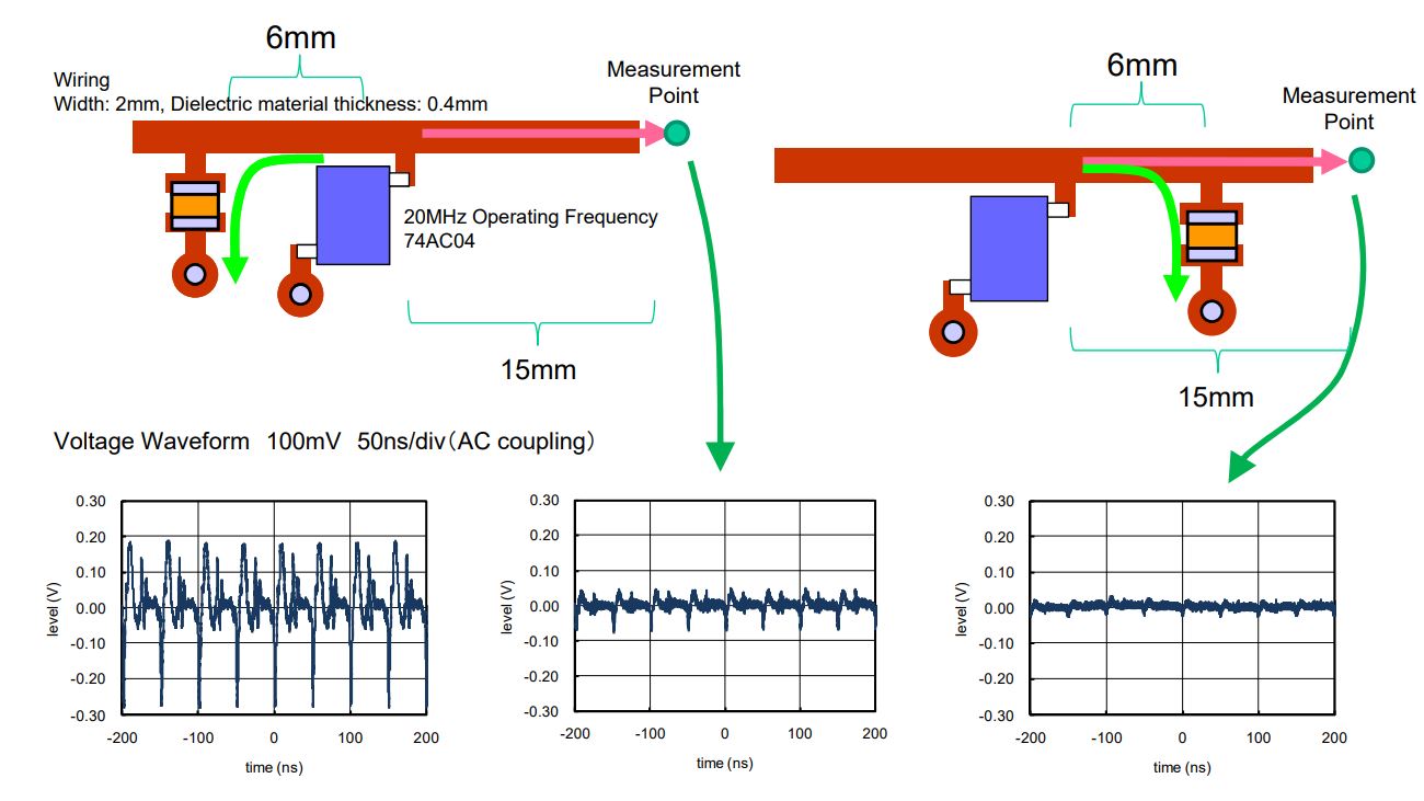
The effect of noise suppression by adding the decoupling capacitor can be conformed by measuring the noise output of various conditions. The experiment and results are reported by Murata. The circuit is operating at 20 MHz, the decoupling capacitor is a SMD 1608 size, 1 uF MLCC capacitor 6 mm from the VCC pin. The waveforms captured by the oscilloscope placed 15 mm away from the VCC pin are shown below from left to right: without a decoupling capacitor, with branched wiring and the capacitor is mounted on the other side of the noise path, and without branched wiring where the capacitor is mounted on the noise path. As the experimental results show the effect of noise suppression is significantly improved by adding the decoupling capacitor and placing it at the right place.