
X-ray is a high-energy electromagnetic radiation with a short wavelength on the scale of 10-12 m to 10-9 m or 1015 to 1018 Hz in frequency. X-ray can easily penetrate an object because of its high energy. When it penetrates an object, the penetration rate varies according to the density and composition of a material, which absorb the X-ray proportionally based on their atomic weight and structure. Optically, the materials made of heavier elements appear darker because of higher absorption rate and materials made of lighter elements look more transparent because of less absorption. Based on this principle, X-ray radiography is now an important instrument and widely used as a non-destructive inspection method in the industry. By using X-ray radiography, we can identify the structure of a gold bond wire and lead frame and accordingly indicate the failure modes inside electronic components and detect defective copper traces on the printed circuit board. It can also identify void distribution in solder balls and soldering defects at SMT (Surface Mount Technology) level by a non-destructive method.
X-ray scanning has been used as a non-destructive inspection method in electronic industry for years. X-ray inspection system provide high precision result of an object’s interior structure without compromising structural integrity. X-ray inspection is often referred as Automated X-ray Inspection (AXI). Modern PCB are usually made for high density of components and of multiple layers. Therefore automated, high-speed, real-time, and non-constructive inspection methods are required for high throughput and reliability. This is especially true for PCBs having area array packages, such as BGA (Ball Grid Array) and QFNs (Quad Flat Packages), as well as flip chips and CSPs, which make solder joints hidden underneath the packages. These situations are commonly found in industrial control, communication, military, aerospace, etc. The solder defects with BGA packages, can be detected by X-ray inspection including bridged balls, tilted BGAs, BGA voiding, insufficient solder, excessive solder, missing balls, poor wetting and misalignment, etc.
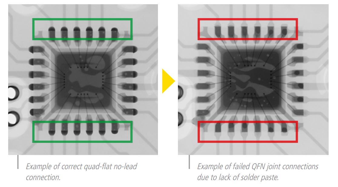
From this figure, the dark black image refers to the material made of heavy elements while the transparent or relatively white image refers to the material made of light elements. Therefore, X-ray inspection is good at inspecting hidden defects including opens, shorts, misaligned, electrical components missing and so on.
Moreover, PCBs with large amount of SMT (Surface Mount Technology) components present challenges for quality inspection because of the smaller leads and packages, hidden solder joints, buried or blind holes compared to traditional through hole components, which only require the conventional inspections tools, such as optical, ultrasonic and thermal imaging, etc. With the trend of continuing miniaturization in electronic components and packages, X-ray inspection method will be demanded more because X-ray technology is capable of penetrating into the inner packaging and inspecting the quality of hidden joints and buried holes. This method of inspection has several industrial applications and is especially useful for industries where quality is the most critical requirement. Manufacturers and suppliers of automotive, aerospace, and orthopedic medical devices benefit from these high precision, non-destructive inspection abilities. With high resolution X-ray technology, inside structure, dimension, failure roots, fit and function can be inspected in a simple process. Imaging out internal features can be the most cost effective and best approach for the visual and dimensional evaluation. X-ray scanning can be used for design verification and evaluating consistency in the pre-production and post-production. When defects are found in the products, locating failure roots without damaging the specimen is possible, which is a significant advantage over other inspection methods. One of the most common analysis that JTL specializes in is void analysis on metal welding components, aluminum castings, electrical components such as printed circuit boards (PCB).
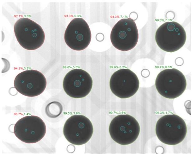
BGA (Ball Grind Assembly) and leadless components impose big challenges for PCB assembly. Therefore, X-ray scanning inspection is required for any hidden defects underneath the board surface. In the above picture, the BGA balls marked in red outline failed the requirements for shape or roundness, which is represented by the first number besides each ball. In the same picture the second number in green stands for the total viding percentage for each BGA ball. Based on the software settings of the inspection system, the operator can set up the acceptable levels and the inspection system can automatically raise the flag of failures.
X-Ray applications in electronic industry:
- PCB surface mount board
- Semiconductor: BGA, CSP, Flip Chip, etc.
- Electric and electronic components
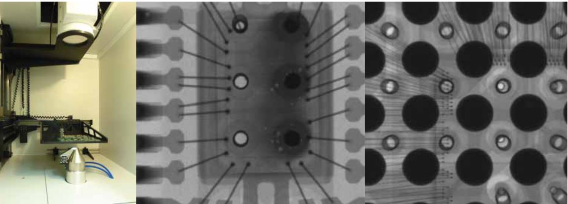
Popular X-ray inspection systems:
![]()
![]()

Reference
- https://www.nikonmetrology.com/en-us/products
- https://www.escatec.com/en
- https://www.tempoautomation.com/
- https://creativeelectron.com/
- https://www.nordson.com/en/divisions/dage/x-ray-inspection
- Krastev, E., Bernard, D., & Nordson, D. A. G. E. (2010, January). MODERN 2D/3D X-RAY INSPECTION–EMPHASIS ON BGA, QFN, 3D PACKAGES, AND COUNTERFEIT COMPONENTS. In SMTA Pan Pacific Symposium.