PCB layout designers have always been concerned about these prominent questions, as how to plan an effective grounding system on the board, whether to route all grounds like analog, digital and power grounds separately or together at the single point and how to eliminate ground loops on the board, etc. EMC (Electromagnetic Compatibility), RFI (Radio Frequency Interference) and EMI (Electromagnetic Interference) are always on the front list of concerns layout designers have. It’s become even more obvious when the component packaging continues shrinking and the density of board components as well as the operating frequency of the system keeps increasing.
Board level EMI and RFI are results of the generation, propagation and reception of electromagnetic energy coupled between components on the circuit board. Therefore, the interferences are highly associated with all the design elements of PCB layout, like, component packages, traces, vias, PCB material and layers, etc. With good understanding of the causes and effects of all the interferences present on the board, the prime goal of PCB layout designers is to eliminate or reduce the levels, paths and sources of interference energy.
Interference noises can be generated by various sources. The input/output (I/O) pins can generate lots of noise. The traces connecting these pins form large antennas. The signals from/to these I/O pins keep changing per the logic and the rate of change is based on the switching clock. The common impedance between the output pin and the clock drivers that are the shared pins supplying the power and return paths causes distortion in the signals. The synchronous nature that all devices in the system operate on the same clock rate causes all current-switching events to occur at the same time, making a large noise spike containing much RF energy. Another source of noise is related to the power management system on the board, which includes voltage regulators and associated bypass capacitors at both the regulator and at the ICs power pins. The power supplies supply the clock drivers in the ICs with the current required for clock switching. The quality of supply output is critical. Also, the oscillator circuit on the board generates noises. The oscillator circuit swings from rail to rail. In addition to the fundamental frequency, harmonics are introduced on the output side because the output buffer is digital that squares the sinusoidal waves. Any noises caused by internal operations such as the clock buffers appear in the output. It’s required to separate the crystal and its tank circuits from other components and traces connecting them on the PCB and reduces the loop areas.
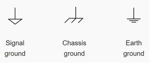
Power supplies especially switch-mode power supplies are serious sources of EMI because of the high switching current flows and sensitive control signals in close proximity. Therefore, careful PCB layout is required to ensure the product to not only operate correctly but also quietly. Among all the considerations of robust PCB layout design, grounding has earned primary attentions. Even though there have been significant confusions about types of ground and effects of ground on circuit, such as circuit functionality, performance and electromagnetic interference (EMI). For PCB layout design, we need to know all the following types of ground.
- Logic ground
- Analog ground
- Chassis ground
- Safety ground
- Earth ground
All signals as well as noises originate from the sources and returns to the ground. The ground symbols in schematics often give the illusion that an unvarying reference ground or equipotential ground actually exists. The reality is that the ground we use as the returns of signals are not an equipotential. The connections from any points on the board to the ground are finite in length thus have resistance (for DC signal) or impedance (for mixed signals). No matter how thick and how short the copper is for your ground traces, it has resistance. The resistance of the ground will cause crosstalk between the two different signals that returns to the same point at the ground. The different currents of the two signals produce different voltage drops and they will be seen as relative fluctuations in the reference. Non-uniform ground potential is the root cause of ground loops.
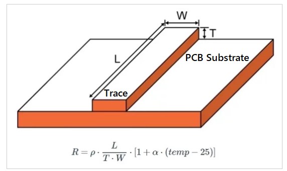
According to the above formula, shorter length of the trace results in smaller resistance, also, thicker and wider traces have lower resistances.
The resistance is temperature dependent with respect to the room temperature at 25 C. If we ignore the temperature dependency, the trace resistance is expressed as R = ρ (L/ (T x W)).
The lower resistance of the ground plane is one of the most important requirements for designing your PCBs. Such PCBs reduce the noises caused by the variations in return currents, and they provide the ground with more acceptable reference voltage to ensure reliable operations of analog circuits.
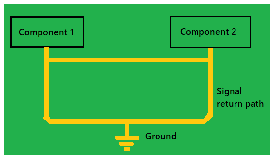
Since the copper traces on PCB have finite resistance regardless of their lengths and thicknesses, any unnecessary shorts along with unexpected sneaky path can form undesirable ground loops as shown in the above figure.
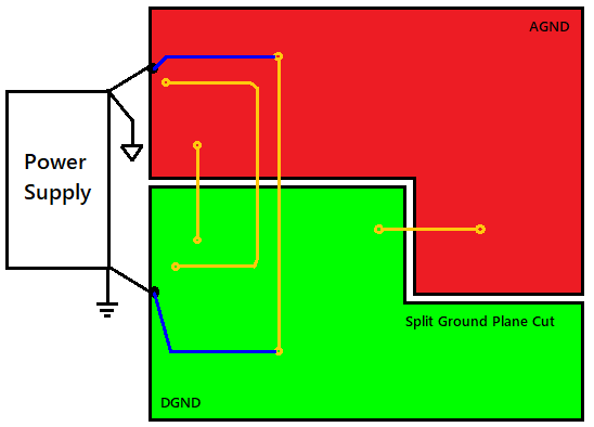
In a mixed signal system, it’s preferable that there are multiple rails for digital subcircuits and analog subcircuits respectively. In many cases, to have separate power supplies for digital and analog sections on a PCB is not possible because of high cost, big board size as well as design time restrictions. Therefore, a common practice is to use a common voltage regulator to generate the needed regulated voltage, e.g. 3.3V or 5.0V for both the digital and analog sections for a single voltage system. In such design, cares to be taken to isolate the analog and digital rails and their respective grounds from each other. This process is called splitting ground. Both grounds must be connected somewhere on the PCB and must be at one place to eliminate any possibility of creating ground loops. The single point grounding scheme forms a star ground structure as shown in the following figure.
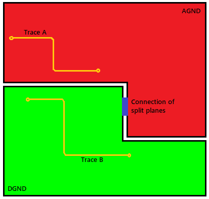
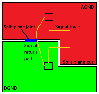
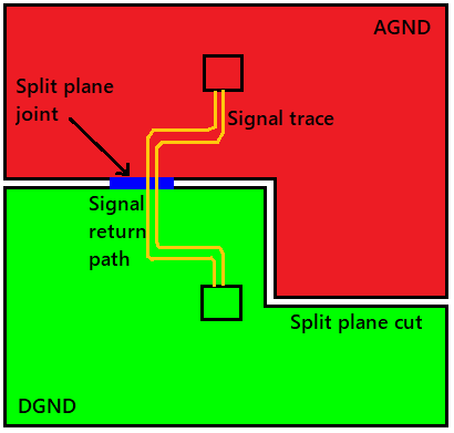
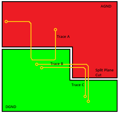
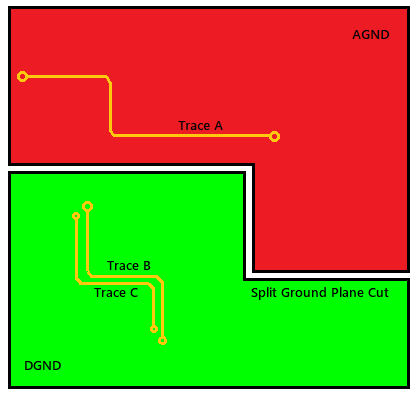
It’s important to properly partition the PCB according to the functionality of either analog type or digital type respectively. Even after we elaborately split the analog and digital ground planes, it may still cause problem by incorrectly placing signal traces. The above left figure shows a situation when we place a signal trace crossover the analog and digital ground planes accidentally ignoring the return path of the signal. We may have learned the fact that the current always takes the least resistive path and the path with least amount of resistance in the above PCB is via the joint point between the two ground planes. Therefore, a large ground loop is created between the far apart signal trace and the signal return path. The solution to this issue is to route the signal trace through the split ground plane joint point as shown as in the above right figure. This way the ground loop can be eliminated.
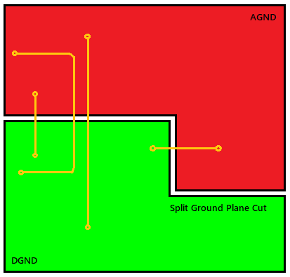
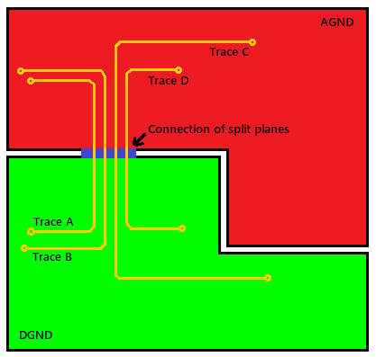
When we split the ground planes for analog and digital circuits, we must connect the two split planes at a single point. Without the single point connection, we have to connect the ground planes at multiple points with ground traces, which can easily create large ground loops as shown in below figure.
This effect good loops will be critical when digital circuits co-exist with analog circuits. The sharing of partial ground plane by an analog circuit with the digital circuits can interfere with the precision analog circuit operations. According to Analog Devices, a 5 cm PCB trace can introduce over 1 LSB (Least Significant Bit) of error in the digitized values generated by a 16-bit ADC (Analog to Digital Converter).
There are ways to reduce the effect of nonuniform voltages across a ground plane. We can use vias or through holes to directly connect the signals to the dedicated underneath ground plane.
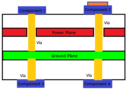
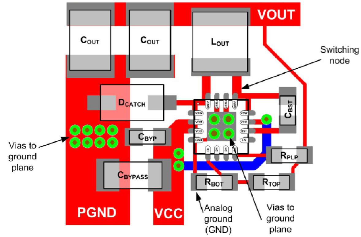
The following example of proper PCB layout with ground considerations for Semtech TS30011 Current Mode Synchronous Buck DC-DC converter. PCB layout for TS30011 must be carefully implemented to minimize EMI for proper operations. Improper layout can cause issues of instability, degraded regulations, noise sensitivity and increased EMI emission. It’s required that sensitive nodes not assigned to power transmission should be referenced to the analog ground (AGND) and should always be isolated from the power ground (PGND). For ICs with exposed thermal pad, a dedicated poured copper area on the component layer for the thermal pad must be provided. Also, multiple vias from this thermal pad solder pad to the underneath power ground (PGND) plane must be placed for effective heat transfer from the thermal pad to the ground plane.
It’s a common practice to have a dedicated ground plane in a four-layer PCB. In many situations, it may be desirable to use the internal layers as normal signal routing, but practically, using one of the internal layers as the ground plane can simplify the ground interconnections by easily dropping vias or through holes directly to the plane to reduce the ground traces and chances of creating ground loops.
The low impedance of the dedicated ground plane is the most important factor for minimizing EMI. When having a single solid ground plane is impossible or costly, it’s common practice to partition the ground plane into several sections to accommodate ground interconnections for different circuits. In this way, the cost of PCB fabrication is reduced while the EMI is also mitigated.
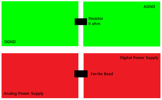
How to connect the digital and analog grounds at one place is the requirements. But different approaches have been taken. As shown below in the diagrams, designers may use a zero-ohm resistor to short the split grounds. Some other designers may use a ferrite bead to make the connection. While these various approaches are possible solutions for some specific applications, it is recommended to not be used generally. Resistors are normally temperature dependent. A zero-ohm resistor may measure zero ohm at nominal temperature. As ambient temperature rises, the temperature change can cause resistance change. The increased resistance in the ground trace messes up the reference of voltages. The impedance of a ferrite bead is dependent on the signal frequency. Ferrite beads are passive components used as low-pass filters that suppress signals with high frequencies. This feature of ferrite beads can be advantageous in pure DC systems, but they can degrade the grounding system when return signals are coupled with large amount of high frequency components.
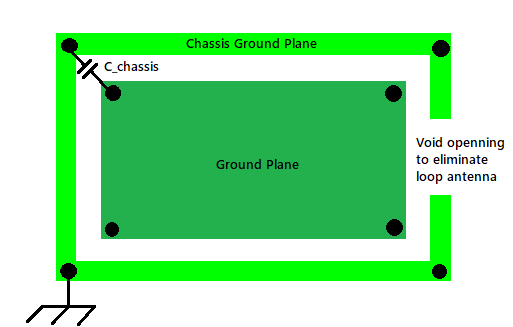
In electronic systems with chassis ground available, whether or how to connect the ground plane with the chassis ground normally raise lots of concerns. Chassis ground is also called safety ground, earth ground or protection earth (PE) under different occasions. As the names of chassis ground indicate, the only function it offers is the safety and protection. It does not play any more roles in the performance or other electronic functions. Therefore, it often not required to be connected to the internal ground plane, e.g. analog ground or digital ground. In some cases, the connection of chassis ground to PCB ground plane is not allowed. In some other situations, when connecting the chassis ground to PCB ground plane is required, some designers just directly connect them at one point via braid cable, mounting screw, or solid copper bar. Some designers may put a ceramic capacitor with low ESR (equivalent series resistance), e.g. 0.1uF, in which case the chassis is not part of the potential reference but is solely used as an EMI dump.
When making connections between the chassis ground and PCB ground plane, it is important to avoid ground loops in several situations.
- Cut voids underneath the magnetics (transformers or inductors), e.g. in RJ45 interface applications;
- Cut the chassis ground to prevent forming a closed loop antenna;
In split ground system, it is important to always keep traces within its respective ground plane; make sure that at any time, there are no traces can cross over the splits (ground cuts) on any layer. The situations when signals cross over the ground cuts are shown below. It is highly possible that ground loops can be created when a trace accidentally crosses over the split ground plane. When signals originating from the interfaces between the analog and digital circuits must be laid out, it is recommended to route them via the single bridging area shown below.
In a split ground system, the traces of analog signals should be placed right above or below the analog ground plane. The similar routing is also applicable to digital signals. This ensures all the signal returns can be made directly to the respective ground planes by vias. This is an effective way to reduce ground loops.
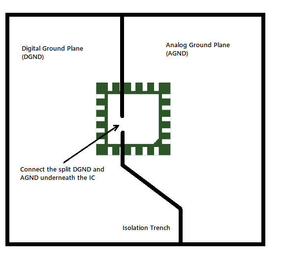
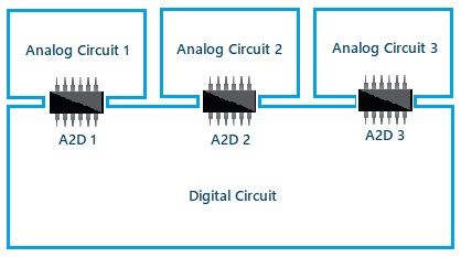
When partitioning the circuit board for analog and digital sections, the split ground is usually connected under or near the mixed signal devices which has both analog and digital rail connections. When making the joint between the analog ground and digital ground planes under the mixed-signal device, it enables running the mixed signals traces with the shortest length and reduce the chance to interfere with other analog or digital signals in the perimeter of the device.
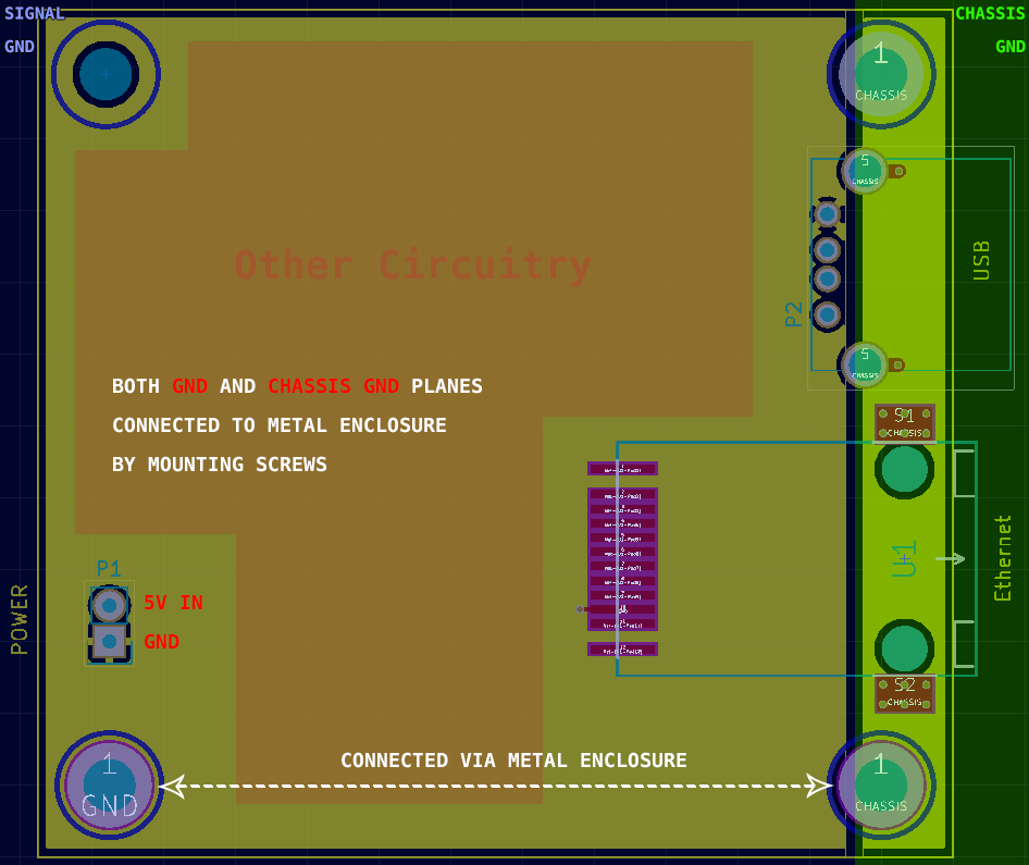
It is common practice to connect the PCB ground plane with the chassis ground and the metal enclosure together with mounting screws. It’s often convenient to make good low impedance connection without using soldered wires but mounting screws. This is especially useful in multiple board stack system within the same metal enclosure as shown in the following figure. The PCB ground plane is connected to the chassis ground via the metal enclosure. With the single point grounding scheme, a good ground system can be created through the PCB ground plane, chassis and metal enclosure for applications in low-frequency domain, below 1MHz, e.g. audio circuit, power supplies. For higher working frequencies, multi-point grounding scheme is required. Under high frequencies, the metal enclosure may show distributive transfer impedance that’s dependent on frequency of the signals. A single-point system cannot get rid of the loop effect. An example of the multi-point grounding system is in the desktop computer. The mother board of the desktop computer has multiple metallic screw holes through which grounding connections can be made via the mounting screws.