All items, like cars, houses, people, books, etc. surrounding us are made of atoms that have equal amount of charge on the nucleus to that on all the electrons orbiting the nucleus. And we know the charge on the nucleus is positive and the charge of the electrons is negative. Overall, the positive charge and negative charge are neutralized. When the atoms are sitting in the state of equilibrium, they have the lowest total states of energy, thus they gain the stability. Sometimes, the atoms absorb energy, and the orbiting electrons can be excited to rise in energy states. When the energy is sufficient and enough, one or more outmost electrons can be kicked off the orbits. This is the process called ionization. The atoms losing negatively charged electrons are called ions and presents positive charge. The stray electrons may go to nearby matters and turn them into negative charge. These standalone charges are so called electrostatic charge. The processes through which ionization can happen include the following triboelectric-charging phenomenon,
- Rubbing the dry plastic surfaces
- Pushing a rim of copy paper along the wooden tabletop
- Taking off a dry wool sweater
- Moving a computer desk along the PET (Polyester) carpet
When two differently charged material get close, it tends to neutralize as much as possible of the total charges they hold. This is the process called ESD (electrostatic discharge). ESD happens very fast and the process can be very intense due to the amount of energy to be dissipated within such a short period of time, which can be some tens of nanoseconds.
Table 1 – Typical voltage level of electrostatic charge caused by human activities
| Activity | Dry | Wet |
| Means of Generation | 10% to 25% RH | 65% to 90% RH |
| Walking across a carpet | 35,000V | 1,500V |
| Walking across vinyl tile | 12,000V | 250V |
| Working at an ungrounded bench | 6,000V | 100V |
| Picking up a polybag from a bench | 20,000V | 1,200V |
| Sitting in a chair with urethane foam | 18,000V | 1,500V |
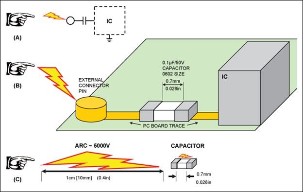
Physics tells that discharge can happen much easily in the air with high humidity. Normally, 5000 V can arc through a small distance of only 1 cm in 50% RH air. Bring this effect down to the PCB scale, which is typically on sub millimeter on component level and micrometer or even nanometer on the IC level. With such a greatly shrunk dimension, the damage caused by ESD can be much easier and bigger. Based on the characteristics of typical dielectric materials, when the electric field established by two oppositely charged surface reaches 40 kV/cm, the breakdown can happen. Let’s assume the 40 kV/cm threshold for breakdown is for a gap of 1 mm between two PCB components. That sets the lower limit of ESD voltage to 4,000 V. We can check it in he above Table 1 and find all the activities in dry air can potentially damage the PCB.
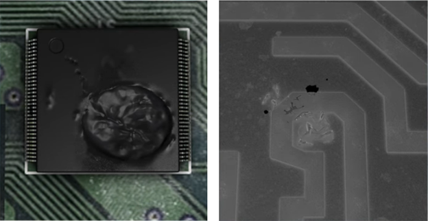
We can look at the following pictures that show how ESD damaged PCB IC component and the inside of the IC die. On the device level with dimension down to micrometers the ESD voltage can caused more direct damage or the threshold for breakdown can be significantly decreased, say several volts. In low power devices, the tolerance for upper limits of voltage can be very little. Therefore, a little above the working voltage can cause catastrophic failures.
There are many examples of PCB board level damages caused by ESD and EOS (electrical overstress). From above description, we know ESD can happen due to many of our activities. In any of these cases, ESD can cause damage if we handle the PCB inappropriately or the PCB has no protection against ESD. The following illustration shows the model of ESD damage.
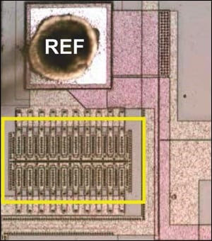
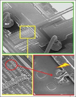
The microphotograph of the inside of the damaged IC with the die being painted with liquid crystal material with pink color when is cool. The paint in the yellow box changed color when applied power to the device. The damaged area was thus identified as the area draws excessive current and heated up more than other areas. The SEM (scanning electron microscope) picture on the right side shows exactly the location of the damage.
As we have observed, the damage to the PCB caused by external high ESD voltages is mostly introduced via the analog input and output interfaces. So, designers have practiced extensively adding various protections to the I/O ports of PCB. There are several models used by rules and regulations for measuring the devices’ capability of withstanding ESD events. We have mentioned the HBM (human body model), one of the three models, namely, HBM (human body model), MM (machine model) and CDM (charged device model). Based on these models, there are three transient immunity test standards documented by IEC (International Electrotechnical Commission).
- IEC 61000-4-2: Electrostatic Discharge (ESD) immunity test
- IEC 61000-4-4: Electrical Fast Transient (EFT) immunity test
- IEC 61000-4-5: Surge immunity test
Based on the test results and practice, we have found many ways to countermeasure the damages caused by high transient voltages, such as grounding wrist strap, antistatic bag, transient absorbing cable, TVS (transient voltage suppressing) diode and EMC compliant PCB layout techniques.
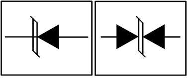
It’s been proved that TVS (transient voltage suppressing) diodes are most effective in protecting semiconductor devices from surge pulses with medium voltage and high energy. The following figure shows the electrical symbols of unidirectional and bidirectional TVS diodes.
TVS diodes has the IV characteristic similar to all other diodes. But TVS diodes are reverse biased for positive transient voltages, so their IV characteristic for positive transient protection mode is plotted in the first quadrant of normal IV characteristic as shown below.
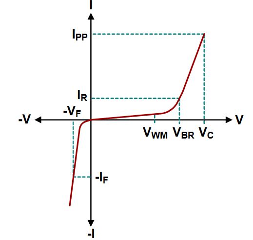
VMM is the TVS reverse standoff voltage, also noted as VRWM that is the voltage where the device only draws the specified leakage current of maximum, say 1uA. This specification can be used for selecting TVS diodes. For unipolar signal, the selection criterion is 0<= Vsignal<=VMM. Under Vsignal, the TVS diode does not impact the circuit performance until the voltage increases further when the TVS diodes starts to work as the breakdown voltage is reached. When the voltage reaches VC, the maximum clamping voltage, the TVS diodes reach their peak specifications, IPP (peak pulse current) and Ppk (peak pulse power).
The TVS diodes look much similar to Zener diodes, but they have different functions as Zener diodes are designed to regulate continuous voltage in normal range (low energy continuous mode) and TVS diodes are used for transient pulse protection (high energy surge mode). TVS diodes are invisible to the circuits being protected in normal operation. They are taking effect when a high energy transient event occurs. To be effective and cost efficient, TVS diodes are made with different specifications, such as different voltage levels, various power rating, mounting options and form factors. By usage, unidirectional TVS diodes are ideal for protecting power rails as well as charging interfaces. The bidirectional TVS diodes can be used to protect any signal I/O ports, such as earphone jacks, BNC connectors.
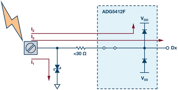
The following protection circuit show how the TVS diode is used to protect high transient voltage attack.

The above figure shows the test results for an 8 kV contact discharge. The TVS diode clamps the high voltage to approximately 54V. The drain voltage of the switch is clamped at only 0.7V above the supply during the transient event. The drain current measurement shows the current flowing through the downstream diodes with a peak of 680 mA during the 60 ns transient. This is equivalent to 1 kV with a peak of 660 mA and a duration of 500 ns based on the HBM (human body model). The protection by a TVS diode is cost efficient and effective.
As we have shown, TVS diodes are good options for protecting high transients, such as ESD for power supplies, I/O ports and high-speed data lines.