In modern power supply design, engineers always face challenges to pushing the limits of many design margins, such as power density, size, and thermal management, etc. As the trend of miniaturization, multiple power rails and high power density continues, new features, topologies, and packaging technologies in power electronics are constantly needed. The high demands of efficient, fast, and cool power switching MOSFETs for mobile devices, telecom device, servers, and networking systems are the main drive for these technology innovations. In recent years, the advancement of semiconductor process technology have helped reduce the on-resistance RDS(on) of MOSFETs to a level that further reduction of the on-resistance is only limited by the device packaging. The industry has seen improvements in performance with various MOSFET packages, such as DPAK, PowerPak, LFPAK, SO-8, CopperStrap SO-8, DirectFET, etc. As the system current demands increase significantly, a new packaging technology is applied. This is called “Source Down” power package, which is different from the conventional “Drain Down” package.
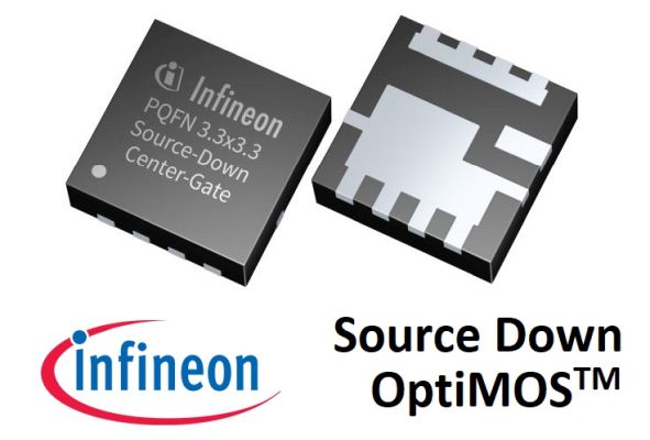
The “Source Down” concept is the new industry standard packaging concept. The first batch of power MOSFETs launched in this package is the Infineon OptiMOSTM 25V in a PQFN (Power-Quad Flat No-Lead) 3.3×3.3mm, which offers small size, minimum package parasitics (especially ohmic resistance) and ultra-low on-resistance down to 0.9 mΩ.
The Infineon Source Down concept on OptiMOSTM is not only a flip chip, but it is a completely optimized package. The optimization of the chip itself as well as the clip results in the ultra-low on-resistance RDS(on) and the significantly reduced thermal resistance RthJC due to elimination of the bonding wires. Power density delivery is one of the most important requirements for modern power management designs. With the reduced on-resistance RDS(on) by up to 30% and thermal resistance RthJC, alongside with the increased maximum continuous and pulsed drain current ID, design engineers are now able to meet the power density requirements. The benefits with the new OptiMOSTM not only include the lower RDS(on), and lower RthJC, but also the layout advantages, e.g., easier paralleling.
Easy Paralleling
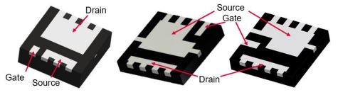
The above figure shows the difference between the conventional Drain-Down package and the two available Source-Down packages, Source Down Standard Gate and Source Down Center Gate. With the Center Gate Source Down package, it’s much easier to connect devices in parallel. The creepage distance is increased to 0.75mm between the drain and source/gate to enable routing the gate signal trace between these contacts, connecting all gate pads of the paralleling devices without need for another PCB layer.
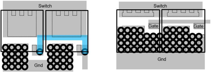
Even though the on-resistance RDS(on) is already significantly reduced, in applications that requires lower on-resistance, device paralleling is the way for further reduction of the on-resistance. With the traditional Drain Down package, the distance between the drain and the source is not enough for routing the gate drive signal underneath the device. In this situation, it is necessary to route the gate signal in another PCB layer as shown as in the above figure by the blue trace.
Thermal management Optimization
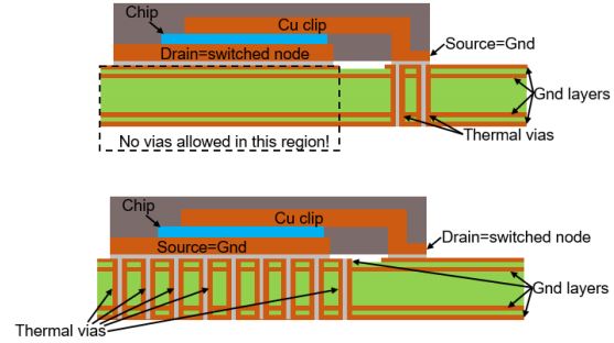
With the Source Down package, the thermal management in ground-referenced systems is much easier and more reasonable. The Source can be connected to all ground planes through thermal vias resulting in a much better and faster heat transfer from the source to the ambient. The effect of Source Down package on thermal dissipation is compared to the Drain Down counterparts as shown in a OR-ing application in below figure.
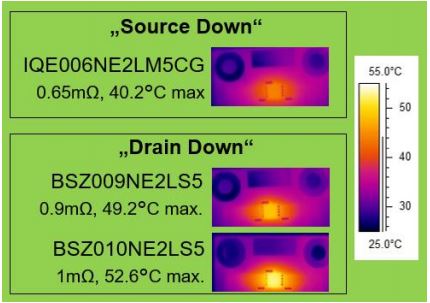
In applications like OR-ing or e-fuse are benefited especially from the low on-resistance RDS(on) of Source Down package because the major loss in these applications are the on-state loss. The above figure shows the Source Down package remains cool at 40.2°C with a 30A load, while the two Drain Down devices heats up to 49.2°C and 52.6°C respectively.
Read more: https://www.infineon.com/cms/media/PMM_3dmodels/innovative-source-down/