

Space travel is so attractive to us while it is so challenging to scientists and engineers. For long time since 1957 when the first space mission was launched, designing device that can survive the extreme conditions in the space has been the priority of any space exploration program. The on-board electronics for space applications presents special requirements for the materials, packaging, components, and protection. The specially designed electronics for space systems, such as the electrical power management and control systems that are capable of all designated functionalities in the ultra-low temperature environments offers lots of advantages over the current systems housed in the “warm box” that utilizes radioisotope heating units to keep the on-board electronic devices at a constant 20 C. Electronic devices that are capable of working at cryogenic temperature can overcome the harsh environment of deep space, shrink the size, reduce the overall weight, lower the power consumption and shorten the development time. From the aspect of performance, power electronics can have higher efficiency at lower temperature than room temperature, which in turn results in optimal device behaviors and fault tolerance in the electrical and thermal properties of the semiconductor and dielectric materials at low temperatures. The Low Temperature Electronics Program at the NASA Glenn Research Center, Cleveland, OH, has conducted a research on devices and systems for planetary exploration and their efficient and reliable performance down to cryogenic temperatures as low as -243°C or 30K. Their research involves characterizing the COTS (Commercial-Off-The-Shelf) components and some developed passive and active devices.
Space environment is hostile to not only human but also electronics. The spaceships must be designed to withstand the ultra-low temperature, vibration at various frequencies, high-g shock, and cosmic radiation. For the temperature, it varies within a much wider range than the operating temperature range for most electronic components have been specified, from -55 to +125°C. For example, the surface temperature pf the Moon ranges from -200°C to +200°C. The following picture shows the temperature contour map of the south pole of Moon.

Some spots of the map show extremely cold temperature. That is because the bottom of the craters in the region of south pole are never exposed to sunlight. In contrast, some peaks and crater rims are exposed to sunlight over 80% of the time, so the temperature is very high on those spots. The LRO (Lunar Reconnaissance Orbiter) on-board Diviner instrument has reported extreme temperatures as low as -238°C (-397°F) within the PSRs (Permanently Shadowed Regions), which is even colder than the surface temperature of Pluto.
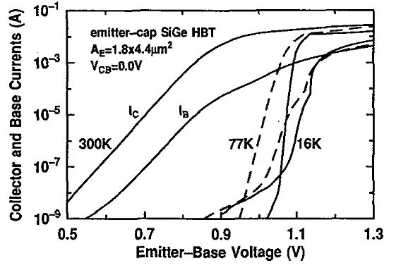
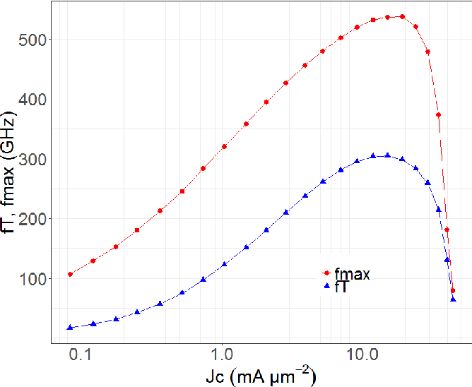
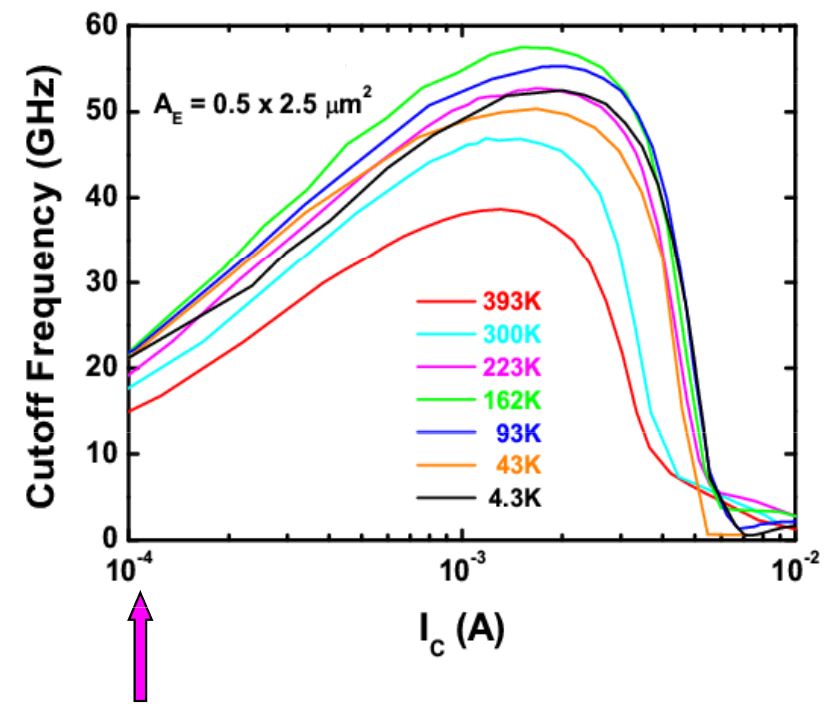
Not only the space exploration presents low temperature challenge to classical electronic devices, but also the modern quantum computing technology requires the core systems to work at cryogenic temperatures. There are many reasons for why we must understand how electronic components and the circuits consist of these components work at such low temperatures. Cryogenic temperature has huge impact to the electronic components, such as the life span and performance. The specially designed COTS components for the specified operating temperature range must be used. It has been reported that at cold temperatures, many characteristics of COTS components are improved as many device parameters saturate below 50 K demonstrating predictable excellent performance. For bulk and SOI Si CMOS devices, the key device metrics, the IDS_Sat, gm, µeff, S and Ioff, etc. improve at low temperature, while VT and hot carrier reliability degrade at cold temperature. The threshold voltage increases at low temperature is because of the increased Fermi potential and expanded depletion region. For bulk and SOI SiGe HBT (Heterojunction Bipolar Transistor) devices, the β, VA, gm, fT, fmax, NFmin improve while β at low currents degrades. (John D. Cressler) In contrast to early SiGe HBTs, advanced SiGe HBTs show excellent potential for cryogenic operations as reported achievements of a fT at 710 GHz and a fmax at 618 GHz both at 4 K, which accounts for a 70% improvement over the reported records at room temperature. Compared to Si based BJTs based on early technology, the advanced SiGe technology has the intrinsic resistance to ionizing radiation due to the fabrication process and the high speed of SiGe HBTs under cooled temperature due to the bandgap engineering.
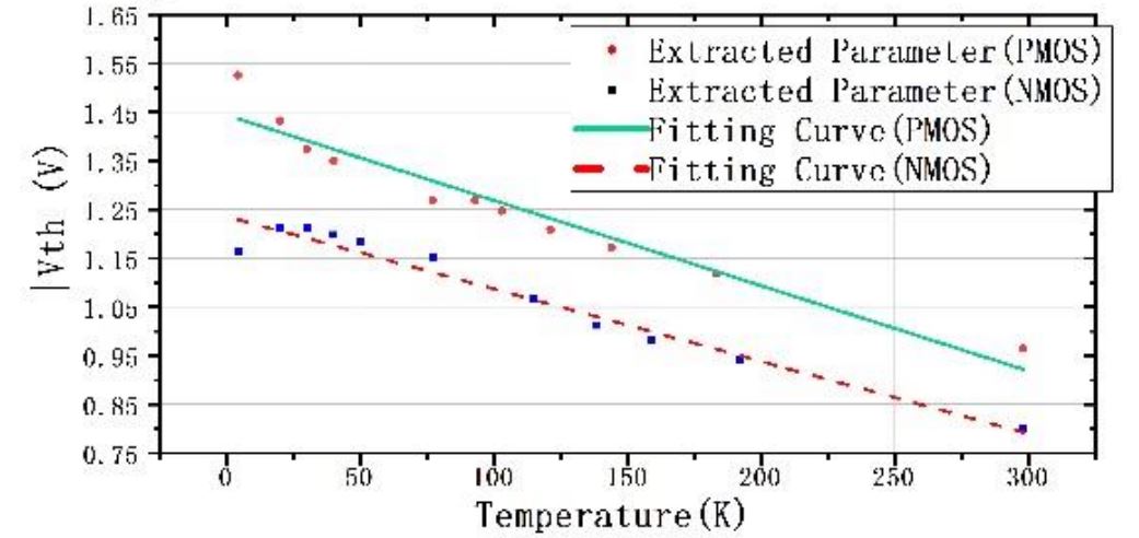
In another study of characterizing 0.18 um CMOS transistors over temperature from 300 K to 4.2 K was reported. In this study, the drain current ID increased with decreasing temperature due to the increased carrier mobility. It also shows the threshold voltage VT increased at low temperature for both NMOS and PMOS transistors. At lower temperature, the carrier mobility is greatly enhanced due to the reduced carrier scattering caused by lattice thermal vibrations.

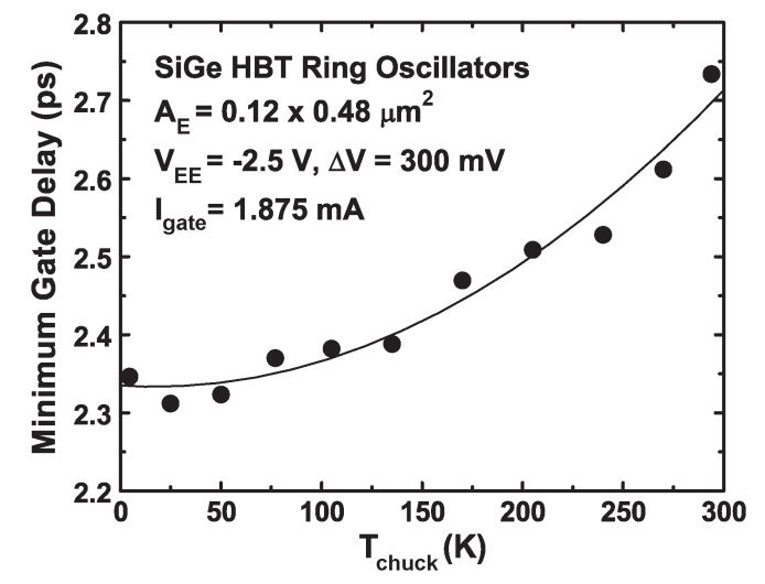
The above plot shows the Measured minimum CML ring oscillator gate delay as a function of chuck temperature. The measurement was achieved on a Lakeshore CPX-HF cryogenic probe station with a temperature sweep from 4.5 K to 294 K. It shows the gate delay of the CML ring oscillator is 2.73 ps at room temperature and the shortest delay is 2.31 ps at 25 K. The improvement is about 15.4%.
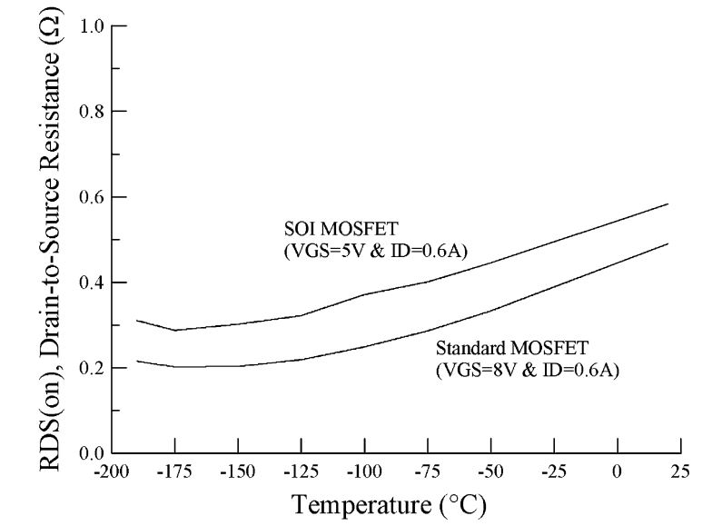
The above plot shows the drain-to-source on-state resistance (RDS(on)) versus temperature for the SOI (Silicon-on-Insulator) MOSFET and the standard MOSFET. The two devices have shown similar behavior in the RDS(on) dependence on temperature. The lowest on-state resistance was recorded at about -170°C and it is found that the on-state resistance tends to increase with further decreasing temperature after -170°C.
Quantum computing is one of the most exciting technological breakthroughs. The two theoretical building blocks of quantum computing are both taken from quantum mechanics, superposition and quantum entanglement. The core element of a quantum computer is called qubits. At least a few thousands and up to several millions of qubits are required for quantum computing and all of these qubits work at deep cryogenic temperatures.

According to John D. Cressler, bulk Si CMOS devices work well at temperatures down to 43K and below. The physical mechanisms of the band-gap engineering are enhanced at cryogenic temperatures.
The improvement of SiGe HBTs performance at cryogenic temperatures is great news. The SET quantum computing readout has several challenges to overcome. The SET devices are highly sensitive to the environment and have low output signals in the 100 pA range. The dry dilution refrigerators have low thermal budgets and imposes serious EMI problems. Also, the large number of leads to and from the device sitting in the fridge are so long that present highly resistive and capacitive characteristics. For long time, silicon JFETs have been the only option for the low frequency and high-impedance readout electronics with very low noise performance (about 1nV/Hz1/2). But these devices cannot operate below 100 K. Therefore, the JFET readout circuits must be separated from the cooled electronics and require long cables to connect them. As the advanced SiGe HBTs are excellent for cryogenic temperature operations, they are considered viable technology for making the amplifiers for SET (Single-Electron Transistor) silicon quantum computing readout. There are several analog amplifiers based on SiGe HBTs have been designed and two topologies have been commonly used now. The SiGe HBTs can provide the best gain vs. power characteristics of any solid-state devices at the working temperature. The design f the amplifiers have used COTS discrete components.
The study conducted by T. Chen and J Cressler et. Al., “CMOS reliability issues for emerging cryogenic Lunar electronics applications” for lunar designing the complex suite of electronics systems used in sensing, actuation, and control of robotic systems provided insight to how reliable the full suite of mixed-signal circuit building blocks can be within operating over such extremely wide temperature range.
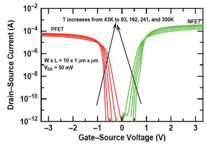
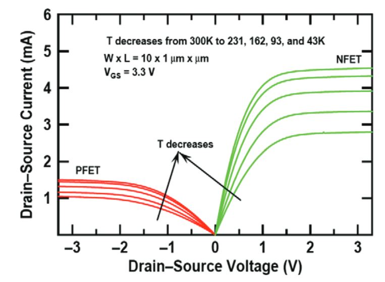
The above two plots demonstrate the typical I-V characteristics of the CMOS deices at temperatures from 43 K to 300 K, with VDS = 50 mV and VGS = 3.3V respectively. At lower temperatures, the current drive capability increases significantly with the same bias conditions. This indicates the performance of the device is greatly improved at lower temperature.

Si CMOS devices present enhanced performance at cryogenic temperatures. At the same time, they achieve the excellent performance at the cost of shorter device reliability lifetime. The degradation of device lifetime can be compensated by using CMOS with longer channel transistors because the long channel length can suppress the hot carrier reliability degradation. The drawback of long channel is the lower W/L ratio that causes lower circuit speed due to the smaller output current driving capability. Therefore, trade-offs must be made between the circuit speed and reliability.
Reference
- Richard L. Patterson et al., “Electronic Components for Use in Extreme Temperature Aerospace Applications”, 12th International Components for Military and Space Electronics Conference (CMSE 08), San Diego, California, February 11-14, 2008
- Del Castillo et al., “Electronic packaging and passive devices for low temperature space applications,” 2018 IEEE Aerospace Conference, Big Sky, MT, 2018, pp. 1-13, doi: 10.1109/AERO.2018.8396521.
- Cressler. Operation of SiGe bipolar technology at cryogenic temperatures. Journal de Physique IVColloque, 1994, 04 (C6), pp.C6-101-C6-110. 10.1051/jp4:1994616. jpa-00253110
- Yuan and J. Cressler et. Al., “SiGe HBT CML Ring Oscillator With 2.3-ps Gate Delay at Cryogenic Temperatures”, IEEE Transactions on Electron Devices, Vol. 57, NO. 5, May 2010
- Chen and J Cressler et. Al., “CMOS reliability issues for emerging cryogenic Lunar electronics applications”, Solid-State Electronics 50 (2006) 959-963
- Manger et al., “Integration of SiGe HBT with fT=305 GHz, fmax=537 GHz in 130nm and 90nm CMOS,” 2018 IEEE BiCMOS and Compound Semiconductor Integrated Circuits and Technology Symposium (BCICTS), San Diego, CA, 2018, pp. 76-79.
- Chakraborty, P.S., et al., “A 0.8 THz SiGe HBT operating at 4.3 K”, Electron Device Letters, IEEE, Vol.35, pp. 151, 153, Feb. 2014
- Luo, Chao, et al. “MOSFET characterization and modeling at cryogenic temperatures.” Cryogenics 98 (2019): 12-17.
- R.L. Patterson, A. Hammond and M. Elbuluk, “Assessment of electronics for cryogenic space exploration missions”, Cryogenics 46 (2006) 231-236