Market-driven requirements for high current, high power and small-size products are in turn driving the engineering designs for new power supply products. The primary design metrics or specifications translated from the vague marketing requirements are the voltage, current and dimensions. From these parameters, we intuitively draw an impression that the smaller the size of the product is, the greater the output power density can be. This vague concept actually can draw an exact math concept:
Power/Volume = Power Density
Or,

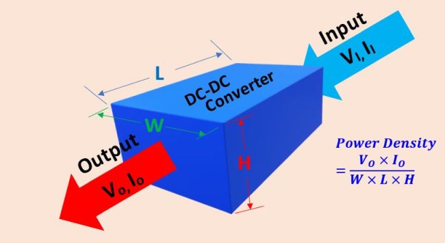
The power density of a DC-DC converter is defined as the continuous output power the converter can deliver in the worst-case scenario. The overall power density is often affected by many factors, such as ambient temperature, operating temperature, altitude and lifetime.
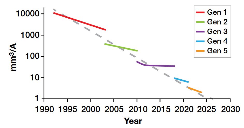
Of course, there are many other requirements, such as output AC ripples, temperatures, transient response, etc., but the power density concept is the primary requirements to shape the engineering designs of modern power supplies. It has been reported that the industry has followed the trend towards high power and miniaturization for years and clearly the trend is continuing. According to J. Morroni and P. Shenoy of Texas Instruments, the reduction in DC/DC converter size for 6A and 10A power modules have been in pace with every single new technology generation.
Technological advancements, e.g., semiconductor material, process, packaging and design, have resulted in significant changes in device size decrease and thus power density increase. The advantages of the power density improvements are enormous to almost all aspects of power supply designs, such as, efficiency, further dimension reduction, cost saving, high component integration and need for novel packaging technology.
Understanding the importance of power density is the first step. To meet the target of desirable power density is the last step. Before we can achieve the goal of higher power density, we must understand the efficiency of the system and all the power losses resulting the lower efficiency. If we look through the history of switch mode power supply (SMPS), we would find that the efficiency was the prior driving force in power technology development. According to Laszlo B.’s article: the development of power density design is hand-in-hand with the improvement of efficiency as shown in the below figure.
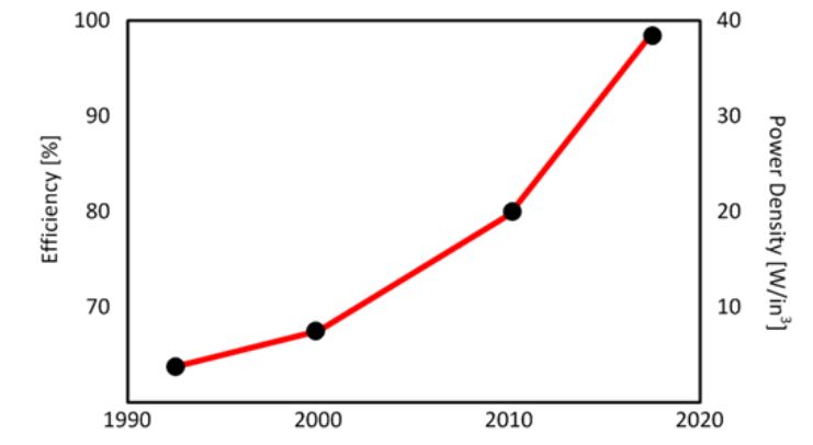
Obviously, achieving higher efficiency of a power system with high or equal power density requires smaller size. Efficiency means less heat dissipation and small size is accomplished by running the switch mode device at higher frequencies.
The inductors in the switch mode converters store and release energy cyclically. As shown by the following equation, the higher switching frequencies the inductor works at, the lower inductance is needed which means smaller inductors.
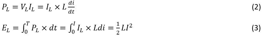
The above equation shows the energy stored in the inductance is proportional to the inductance. The larger the inductance the more energy the inductor can store. We can also find the equation to calculate the inductance L by using the duty cycle, voltage, switching frequency and the current change in the switching cycle:


The size shrinkage enabled by higher switching frequencies is better illustrated by the above figure. The other benefits brought by shrunk size include the increased control loop bandwidth for better transient response with less output capacitance.
While increasing the switching frequency results in small device size, the higher frequencies also cause switching loss and heat dissipation for performance derating.
For a high side MOSFET switch, the power dissipation of the switch during the transitions from OFF State to ON State and vice versa.
The switching begins when the VGS of the high-side MOSFET is greater than the threshold voltage VTH and the current begins to flow to charge the input capacitance CISS. The energy stored in the output inductor is calculated using equation (3).
The power loss due to switching is calculated by the following equation:

Where, IDS is the Drain-Source current, VDS is the Drain-Source voltage, trise is the rise time of the output voltage, tfall is the fall time and fswitching is the switching frequency.
The efficiency of MOSFETs consists of two types of losses, the conduction loss and switching loss. Simply, the total power loss is to combine the conduction and switching losses. The switching loss is the dominant loss type at high frequencies.
The heat dissipation is mainly caused by the conduction loss of the MSOFET. One of the most important parameters of the MOSFET is the on-resistance RDS(on). The way to find the conduction loss is straightforward by using the Ohm’s Law.
Where, D is the duty cycle, Io is the output current, II is the input current, Vo is the output voltage.
There is another type of loss called gate charge loss that is related to the gate charging process of the MOSFET. The gate capacitance is formed by the metallic deposition layer and the conduction channel which are insulated by a layer of SiO2.
![]()
The loss caused by the gate charging is more significant at higher switching frequencies.
There are other losses, such as switching, conduction, dead time and gate charge losses on the low-side MOSFET if the H-L side topology is used, as well as the drain charge loss. For simplicity, we only considered the switching, conduction and gate charge losses.
When we are putting much effort in reducing the power losses, we cannot ignore another key performance that can be the limiting parameter for meeting the ultimate design goal. That’s the thermal management. The losses are transferred into heat and the heat accumulation inside the device must be removed as fast as possible to keep the device performing well. The removed heat goes to the ambient. The model of device thermal resistance show the thermal behavior of a semiconductor device is similar to that defined by Ohm’s Law. Therefore, we have the thermal resistance parameters listed in the device datasheets, such as RθJA (°C/W) – junction-to-ambient thermal resistance and RθJC (°C/W) – Junction-to-Case thermal resistance. These parameters determine the thermal behavior of the devices and they are dependent on the packaging design. The goal of thermal optimization by packaging, PCB, heatsink, etc. is to slow down the temperature rise caused by the power losses, such as conduction loss, switching loss and gate charge loss, etc.
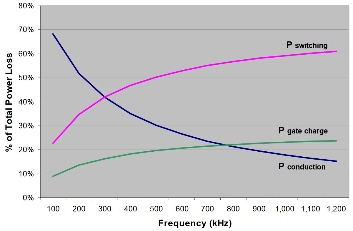
As we have analyzed, there are multiple factors in the play with the power density design. In cases, we just need to optimize one or two factors to gain significant boost in performance. For example, when we tackling the switching frequency, we must understand how changing the switching frequency will affect the performance and interact with other parameters. Lower frequencies mean less switching loss, but they also mean larger magnetic components, higher cost, and big sizes. The below plot shows that as we increasing the switching frequency, the switching loss and gate charge losses increase, whereas the conduction loss decreases. The goal of the frequency optimization should be existing somewhere between 200 kHz and 500 kHz.
Of all the consideration discussed, the efficiency should be the primary factor in power density optimization. When the power density is increased, the rest we must do is to innovate the packaging for better thermal performance and optimization for design parameters and component selection. The items on the checklist of the design project must include:
- Reduce the losses – switching and conduction
- Topology and control selection
- Assembly – optimization of components, cost, size, and new technologies
- Thermal management