As the awareness of environment protection keeps increasing, there is more investment put in the studies of new energy, clean energy, renewable energy, and new technologies for high-efficiency power conversions to help further reduce wasted power. In the field of power electronics, researchers have discovered many new materials, device configurations and novel topologies. The WBG (Wide Band Gap) materials, SiC (Silicon Carbide) and GaN (Gallium Nitride), show unparalleled promise of making next generation of high performance devices in power conversion for EVs (electric vehicles), renewable energy, cloud computing, fast charging stations, and 5G communication, etc. Use of WBG devices in energy infrastructure offers great efficiency, improved thermal performance, compact size, light weight, and reduced cost.
The switching loss of power devices accounts for a large portion of the total loss in power conversion. Therefore, use of low switching loss semiconductor devices can achieve high efficiency in power conversion. Currently, we are still largely using the conventional silicon-based power devices, Si MOSFETs (Metal Oxide Field Effect Transistors), IGBTs (Insulated Gate Bipolar Transistors) and thyristors. The limitations of semiconductor devices based on Silicon is well known:
- Low bandgap of 1.1 eV and low breakdown field of 30 V/um, which require high device thickness for high voltage applications.
- Low frequency in switching because of conduction loss of Si based devices, which require large die areas to keep the resistance low.
Compared to the conventional Si based devices, the SiC and GaN devices have many advantages.
- High bandgap (3 eV for SiC and 3.4 eV for GaN)
- High thermal conductivity
- High breakdown field (about ten times higher than Si)
- Stable on-resistance with respect to temperature
- High electron mobility (double that of Si)
- Low output charge and gate charge (ten time lower than Si)
- Near zero reverse recovery charge (good for high frequency switching)
On Semiconductor as a leading provider of power management products, has been dedicated to the development of a full line of WBG (Wide Band Gap) power devices including SiC diodes and MOSFETs, GaN HEMTs (High Electron Mobility Transistors), SiC and GaN drivers and integrated modules.
On Semiconductor SiC Device Offer the following outstanding characteristics:
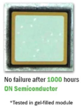
Highest reliability ensured by the patented termination structure
- H3TRB Testing results (High Temperature/Humidity/Voltage/Reverse Bias), 85C/85% RH/85% V (960V)


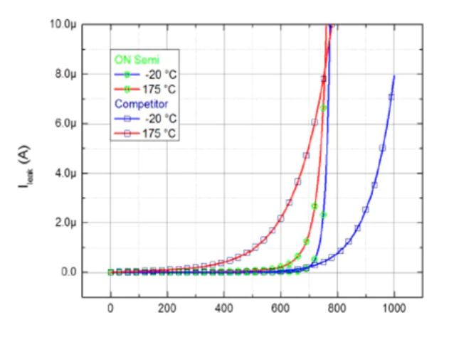
Robustness – SiC Diodes Reverse Leakage

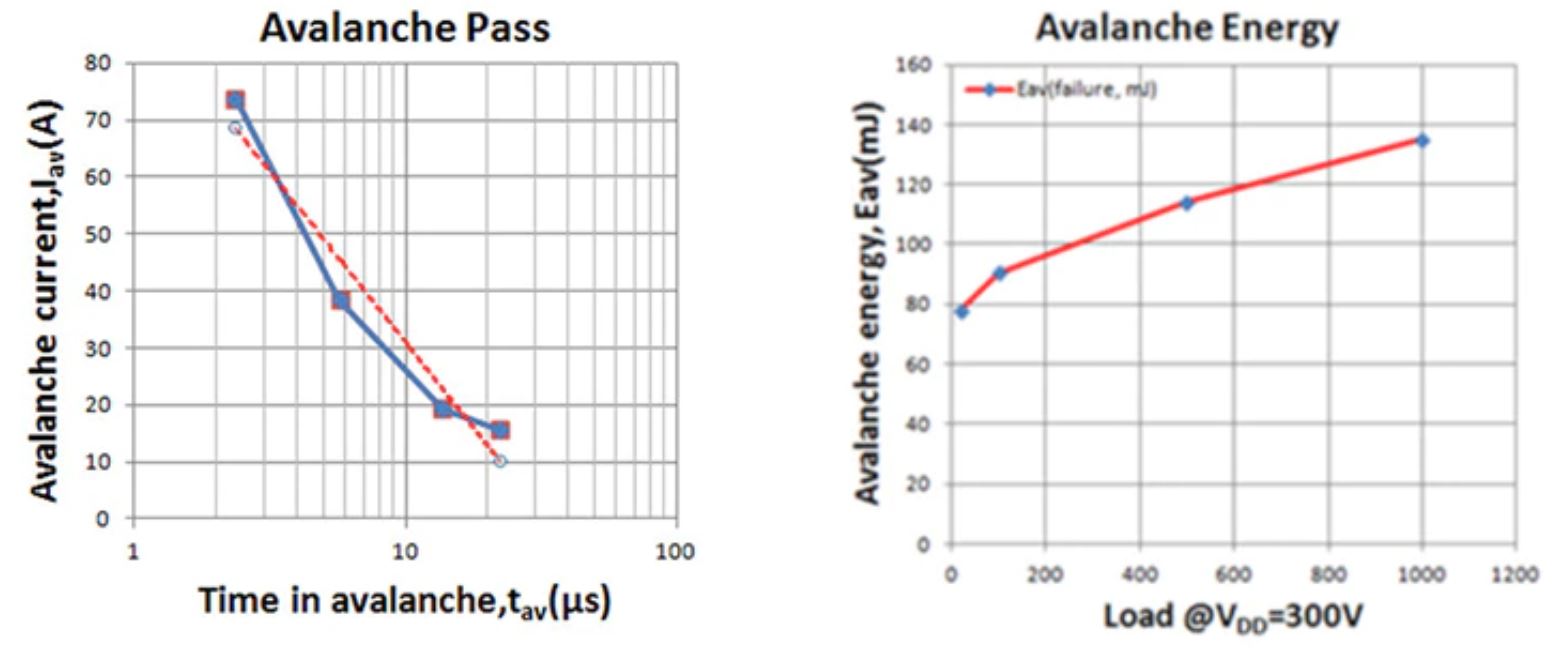
Ruggedness – SiC Diodes Surge and Avalanche

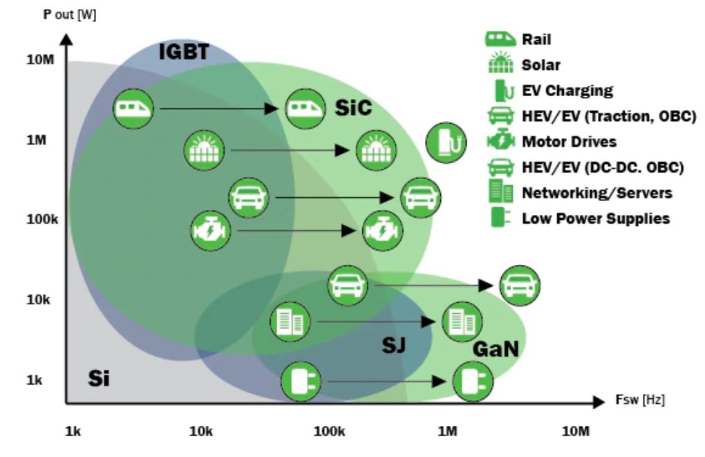
Applications of WBG (Wide Band Gap) Devices