Low dropout voltage as the name of LDO regulators tells, is the most important performance measure of the device and is always included in the datasheet. Low dropout voltage indicates low power consumption by the regulator thus ensure largest power delivery to the intended loads. For more and more portable devices that run on batteries, this is especially important because for many of these devices, the batteries are supposed to keep powering the device for years down the road or it’s just impossible to replace the batteries during the life of operation of these devices. To extend the battery life has become critical. LDO regulators have been popular in such applications due to the small dimensions, less cost and high efficiency. With new technologies, modern LDOs also provide characteristics of low quiescent current, low input noise, wide ranges of input and output voltages. Some have integrated with advanced protection features. Low quiescent current is another important parameter that indicates the current draw by the device when there is no load or light load condition. Low quiescent current offers two folds of advantages. Typically, LDOs are required to work continuously with high load as well as low or no load, therefore, a low quiescent current of the device means low power consumption under low or no-load conditions. Also, most of the wireless and portable devices, such as wireless sensors and IoT nodes are working on duty cycles, meaning that they spend lots of time in sleep mode when the load current is cut down to zero. For battery powered applications, the quiescent current of LDOs should be as minimum as possible to preserve battery life for portable devices.
LDOs have found applications in IoT, sensor nodes and medical devices which require stable and noise-free voltage rails for microprocessors, FPGAs and ADC reference voltage source. Before we start designs of LDOs for our applications, we got to understand the operation modes of LDOs.
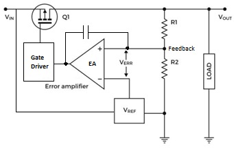
As shown in the above simplified LOD circuit, the input current and voltage are IIN and VIN respectively, which gives the input power of the LDO: PIN = VIN x IIN. When the device is turned on, it delivers the output current IOUT and output voltage of VOUT to the load. The output power the load receives is therefore POut = VOut x IOut. As we find in the above simplified internal circuit of LDO regulator, the only component in series with the load in between of the input and output voltage is the pass FET. Therefore, we should be able to assume IIN = IOut.
Therefore, if there is no voltage drop (VIN-VOut) between the input and output, we would get no power loss, since PLoss = 0 = PIN – POut . But in real world, VIN is not equal to VOut. In other words, we have a voltage drop between the input and output. In all applications of LDOs, we cannot eliminate the power loss because of the voltage drop on the pass element. When we use P-type devices, the voltage drop of can be very small because of the much reduced ON-state resistance, RON, Vdropout = IOut x RON
When the LDO is set to shutdown mode, it stops delivering power to the load by cutting off the load current. In shutdown mode, the shutdown signal is received to drive down the internal circuits of the LOD regulator, such as the clock generator and output discharge. The current draw of the LDO in shutdown mode is called shutdown current. The power loss in shutdown mode is PLoss = IShdn x VIN.
Besides the above two modes, the LDO can also operate in standby mode when the LDO is enabled but no load current is supplied to the load. The current draw in this mode is called the quiescent current. During standby mode, the LDO regulator still needs to regulate the output voltage by drawing a small amount of current, the quiescent current, to activate the internal circuitry. The power loss in this mode is PLoss = IQ x VIN
After we understand the working modes of LDO, we can find the best use of LDOs in IoT applications. An IoT application is normally working in discontinuous style with designated ON and OFF duty cycling. In many applications, the designers may not want to turn the device off while in waiting period. Instead, the device can be switched to sleep mode to save power and gets awaken up when it’s needed. In the sleep mode, the LDO is not active, but maintains the output voltage regulation with zero load current. The only current draw is the quiescent current needed to maintain the internal circuitry active. For many IoT applications, the waiting period or sleep mode may make up to 90% of the time, which means we can save 90% or more power if we simply turned the device off in this period. As we have demonstrated above, the current draw of the device in sleep mode is the quiescent current. Since the quiescent current is the only current draw in more than 90% of the time, its impact to the battery life becomes the main concern about the performance of the device. Even though the quiescent current is very small, the long-term effect is to drain the battery at a much reduced rate compared with the full load current.
Here, we take TI’s TPS76933 LDO as an example. Assume the input voltage VIN is 5V, the output voltage VOut is 3.3V at 100mA load current and the no-load quiescent current IQ is 17uA, shutdown current IShdn is 1uA.
The power loss of TPS76933 when it’s activated to power the load at 100mA is:
PLoss = Vdropout x ILoad = (5 – 3.3) x 100mA = 170mW
If the TPS76933 is turned on all the time, the power dissipation will be maintained at 170mW. That power loss is quite large for the devices using battery as the primary power source. If we turn the device off when it’s not needed, we can cut the current draw down to the quiescent current, 1uA.
PLoss = VIN x IQ = 5V x 17uA = 85uW
The ratio between the two power dissipations is 2000! What a big difference it can create by cutting off the unnecessary power loss. Since we have shown the quiescent current makes the biggest impact on the power consumption of the IoT device, we must understand selecting an LDO with even lower quiescent current can further reduce the power consumption.
If we go further by shutting down the LDO, we can reduce the current draw down to 1uA and the power loss is PLoss = VIN x IShdn = 5V x 1uA = 5uW. But keep in mind that completely shutting down the LDO may not be feasible and the effect of long turn-on response of the device may significantly impact the performance of some applications.
LDO regulators consists of a PNP BJT or a PMOS as the pass element. Due to the low saturation voltage of P-type devices, the LDOs can be made to have as low as 100 or 200 mV voltage drops. Some ultra-low power LDOs have voltage drops less than 100 mV. The obvious advantages due to ultra-low dropout voltage include low heat dissipation, good line regulation, good load regulation and low ripples, which are among the requirements for the power supplies of IoT devices.
We now understand how much power is dissipated by the device for each operation mode. The other consideration is then the heat generated by the power dissipation.
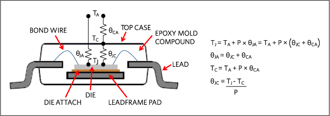
Based on the generic model of an LDO regulator, we have the power dissipation PD:
PD = (TJ – TA)/θJA
PD is the power dissipation in watts (W)
TJ is the junction temperature rating (°C)
TA is the ambient temperature (°C)
θJA is the thermal impedance from the junction to ambient (°C/W)
The above equation indicates the thermal performance of the device is dependent on the device material and package, as well as the ambient temperature. The equation can be used to calculate the heat dissipation based on the selected device with specific package under certain ambient temperatures. If we transform the the above equation into the following form, we can use the result for selecting the right device with desirable package.
θJA = (TJ – TA)/PD
Let’s give an example using TI’s 3.3V ultra-low power LDO TPS 76933.
VIN = 5V + 5%
VOut = 3.3V +/- 2%
IOUT = 100 mA
TA = 50C, free air flow
PD,max = (VIN – VOUT) x IOUT = ((VIN x 1.05) – (VOUT X0.98)) x IOUT = (5.25 – 3.234) X 0.1 = 0.2016W
θJA, max = (TJ,max-TA)/PD,max=(150 – 50)/0.2016 = 496 °C/W
Therefore, to meet the thermal dissipation requirements to keep the device cool enough, we need select a package of TPS76933 so that its θJA is less than the θJA, max.
θJA <= 496 °C/W
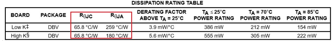
From the datasheet of TPS76933, we found only DBV package is available for selection. The DBV package (SOT-23) on either Low K or High K board can meet this requirement, as the θJA for each case are 259 °C/W and 180 °C/W respectively.
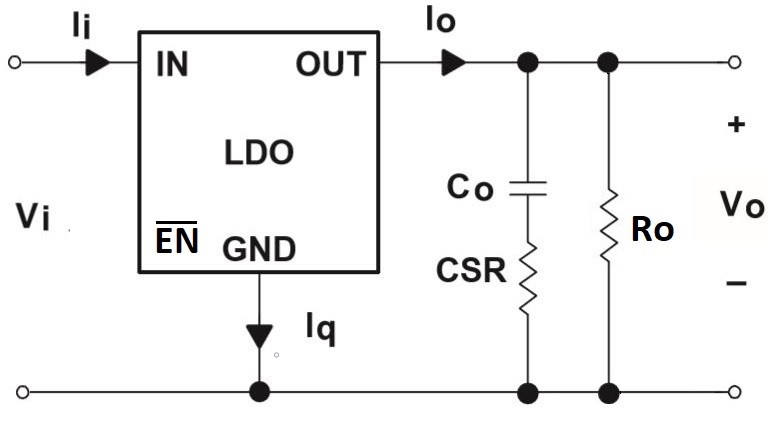
The simplified thermal impedance model from Maxim Integrated for industrial standard IC package is shown below. We know the thermal resistance between the device junction to the ambient is made of two components, the junction-case thermal resistance and case-ambient thermal resistance. The two parameters are usually listed in the datasheet of the component.