Modern electronic devices are designed based on optimization of size, power and functions. Power efficiency is one of the primary considerations of the design engineers. This is especially true for portable electronics that run on batteries, like smartphones, cameras, laptops, tablets and various industrial equipment. Even though many electronic components have been made extremely power efficient, they still consume even in “sleep mode” or stand by. In such a case, we would like to have a “switch” that can automatically turn the supply rail off to save power and turn it on when the device wakes up. The switch would also automatically cut off the device from the power supply to protect it from damage during abnormal power situations, such as a power surge, an electrical transient or an insertion or removal of the battery.
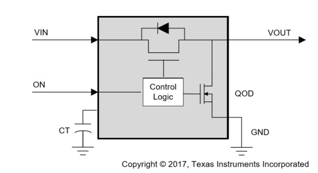
Load Switch block diagram

A load switch can be either a circuit that consists of discrete components or an integrated circuit. As the block diagram shows, the core of a load switch is a MOSFET that is usually an enhancement mode type) as the power pass element. The MOSFET connects or disconnects the load to the power by a control signal from the control logic circuit. The control signal drives the MOSFET gate circuit to turn the MOSFET on or off. Of course, a practical load switch includes more features and functionalities than those illustrated by the simplified diagram. Generally, a load switch contains the following functional parts:
- Pass MOSFET: it is the core of the load switch that determines the voltage and current ratings the load switch can ultimately handle. One of the key parameters of the MOSFET is the ON-state resistance that determines the maximum power dissipation of the load switch.
- Gate driver: it controls the gate of the MOSFET via the control signal from either a microcontroller or an analog circuit. The gate driver circuit also determines the rise time of the load switch, which is an important parameter.
- Control logic: this circuit is driven by a signal from an external source. The control logic controls the load switch to turn on or turn off in a controllable way. The control logic also controls other functional blocks, such as the Quick Output Discharge (QOD), charge pump and protections.
- Charge pump: this functional block is only needed by an N-channel MOSFET because a certain level of positive voltage between the gate and the source is needed to turn on the MOSFET.
- QOD (Quick Output Discharge): QOD is a resistor between the output pin and ground and is turned on or off by a MOSFET. It turns the resistor on wen the device is disabled via the ON pin. The QOD can rapidly discharge the output pin to prevent the output from floating when the output is cut off.
- Protection: it includes thermal shutdown, inrush control, reverse current protection, current limiting, overvoltage and undervoltage, etc.
How to interpret key parameters from the datasheet:
Input voltage range: VIN, the maximum input voltage allowed by the device is one of the important parameters to consider when selecting the load switch. This is the limit of the input DC voltage not only for the steady state operation, but also for any possible transient spikes.
Bias voltage range: VBias, some types of load switches require a bias voltage to turn on the FET or maintain minimum functionalities of the internal circuitry. This bias voltage is independent from the input voltage.
Maximum continuous current: IMAX, the maximum current rating is one of the important parameters to consider for device selection. It should be higher than the peak currents for steady state as well as transient mode.
ON-state resistance: RON, it is the total measured resistance from the VIN to the VOUT pin of the load switch. A load switch has many components that contribute to the total resistance of the device. It’s a combined effect and determined by many factors. Adding the load switch to the power path causes a voltage drop, Vdrop = VIN–VOUT = RON x ILOAD
Quiescent current: IQ, the quiescent current is consumed by the load switch when the switch is turned ON but there is no load on the output. The quiescent current is combined with the ON-state resistance loss to determine the total amount of power dissipation by the load switch. Generally, the part of power loss due to the quiescent current is negligible if the load current is large enough.
Shutdown current: ISD, the shutdown current draw is the amount of current flow through the ON pin when the device is disabled and there’s no output current. When the load switch is disabled, there is a small amount of leakage current by the pass FET. Also, some controller circuitries such as protection circuits are still on and take some amount of current. They combine to make the total shutdown current. The power loss due to the shutdown current is still much less than the amount saved by turning off the load with the load switch during standby mode.
Rise time: tR, the rise time is different from device to device. The rise time determines the slew rate of the input and the inrush current that is inversely proportional to the rise time.
Useful calculations for load switches
Voltage drop
The load switch is a device used to turn the power rail on and off when it is needed. The load switch is an insertion into the power path between the source and load. Therefore, it is important to understand what this insertion can impact the device’s performance. The fist step is to know the voltage drop caused by the ON-state resistance of the pass MOSFET. Since there is always a finite resistance of the MOSFET, a voltage drop on the pass FET is inevitable. Now the key is to know how much the voltage drop is acceptable for the expected performance of the load switch based on the application requirements. The greater the On-state resistance, the higher voltage drop is:
![]()
Where:
ΔVmax is the maximum voltage drop on the pass FET, ΔVmax = VIN – VOUT;
ILoad is the load current;
RON,max is the maximum ON-state resistance of the pass MOSFET at a given input voltage VIN;
If the application requires to control a large load current, or the power rail to be switched is low, then the dropout on the pass FET must be as small as possible. In this case, the ON-state resistance of the MOSFET needs to be as low as possible.
In other applications, if the pass current is low, then a MOSFET with average ON-state resistance may be a good choice as the cost of such a device is typically lower than a low ON-state resistance device as well as the reduced die size and package.
Inrush current
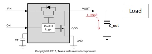
The load capacitor between the output pin and the ground pin can impact the transient behavior of the device. When the power is turned on, the output begins to ramp up to the targeted regulation voltage and charge the load capacitor rapidly. When the capacitor is being charged up, the input rail may dip because of the high inrush current via the load capacitor. If the voltage drop is so large that it drops below the brownout thresholds of the components connected to the power rail, they will reset and may cause the entire system to enter an unpredictable state. If the load capacitor is large, it may cause a shorted load during the short period of inrush. Moreover, if the inrush current exceeds the current ratings of the PCB traces and connector pins, damage may be resulted. Control of the current ramp rate can resolve this issue. It is a very useful application of a load switch to control the amplitude of the inrush current when the device is commanded to turn on.
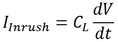
Where:
IInrush is the inrush current through the load capacitor CL;
CL is the load capacitor
It is shown by the above equation that the inrush current is proportional to the rate of output voltage change. Therefore, the way to control the inrush current is to limit the current change by increasing the rise time of the switch. When the load capacitor is slowly charged when turning on, the peak current is reduced. In other load switches that have current limiting function, the device can automatically enter the mode of current limiting when it is turned on, so that the load capacitor is charged up with the limited current.
Power dissipation
The power dissipation is one of the most important considerations in selecting the load switch. As a pass element, the load current passes through the load switch thus a power loss due to the ON-state resistance is generated:
![]()
If the ON-state resistance is small, the power dissipation will generate little heat to cause a significant temperature rise. This is the case that the load switch is used for normal operation. For abnormal situations, like short-circuiting or overcurrent events, the load current will be so large that the power dissipation may be over the limit causing damage to the device. In such a case, a load switch with current limiting can meet the need.
When we use a load switch with current limiting function, we must pay attention to a situation that the device may get into cyclic thermal shutdown and eventually fail in a short-circuit event. When the load is shorted to ground triggering the current limiting protection. The output current is limited to a preset constant current and the power dissipation is at a high level to cause a thermal shutdown. When the temperature drops, the device restarts and encounters the short circuit condition again. So, the thermal shutdown gets activated. This process will cycle itself again and again until the device fails with a thermal overstress or the device is disabled. For better protection, some load switches have integrated with automatic restart feature and programmable current limit using an external resistor.
As discussed, quiescent current of load switches may be significant in some cases as shown by the following equation:
![]()
Under the condition as the load current is large enough, we can ignore the power loss due to the quiescent current.
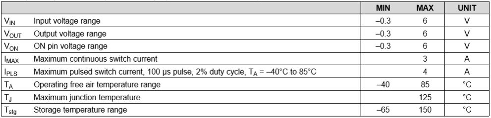
Thermal Considerations
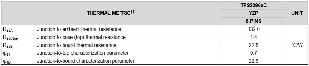
Power dissipation of a MOSFET will cause its junction temperature to rise and can affect its performance. The lifetime of the device is also dependent on the junction temperature. Three of the most important thermal specifications of the load switch are the maximum operating junction temperature, TJ,max, ambient air temperature, TA and the thermal resistance from the junction to the ambient air, θJA. The typical thermal specifications of a load switch (TI TPS22963C) are shown in below table. Therefore, the maximum power dissipation of the MOSFET can be determined by the following equation:
![]()
For example, the thermal resistance, is 132 °C/W, and the maximum junction temperature, is 125 °C, if the ambient temperature is 70 °C, than the maximum power dissipation will be limited to PD,max = (125-70)/132 = 0.417 W.
As described above, the power dissipation depends on the ON-state resistance of the MOSFET, and the ON-state resistance increases as the temperature increases. The maximum allowable junction temperature is important in determining the maximum power dissipation capability of a load switch. When the maximum allowable junction temperature is over the specified limit based on the designed maximum output current, an effective cooling method can be used to improve the thermal capability, such as a heat sink.