One of the most important characteristics of MOSFET (Metal-Oxide-Semiconductor-Field-Effect-Transistor) is the resistance between its drain and source when it’s turned on. This characteristic is normally written as RDS(on). When MOSFET is used in power applications, such as power switches, ORing multiplexer, DC-DC converts or load switches, the RDS(on) is the determinant of the maximum current and power ratings of the MOSFET when the working voltage and thermal management are kept the same. The lower the RDS(on) value, the higher current it allows to conduct when it switches on.
Thanks to the advanced MOSFET Trench technology, very low RDS(on) and low gate-source voltage can be achieved. With the trench technology, shortly trench gate architecture, the MOSFET’s gate electrode is buried in the trench etched in the silicon to form a vertical structure, which allows the current to flow vertically from one surface to the other surface. This feature enables trench MOSFET to have much higher current drive capability. Comparing to the conventional planar MOSFET, the trench gate MOSFET also has drain, source and gate structures, which are constructed in such a way to allow vertical current flow. With multiple trench MOSFET cells connected in parallel, the Drain-Source on Resistance RDS(on) is greatly reduced. The following diagram shows the cross-sectional structural difference between a trench structure and a conventional planar structure.

As demanding for higher efficient power supply as well as longer battery life for mobile applications continuously increases while devices with conventional structure is fast approaching their design limits, lowering RDS(on) has become one of the most challenging tasks facing semiconductor industry. Emerging recently, trench MOSFETs have the lowest RDS(on) that makes power MOSFETs greatly efficient and optimal in reducing the losses in conduction and switching. As an example, MagnaChip’s new single 30V N-Ch trench MOSFET, MDU2511S, can deliver 188A at 10V VGS (Gate-Source voltage) and 96.2W power dissipation. The maximum RDS(on) at 25°C is merely 1.7 mΩ (VGS = 10V, ID = 22A).
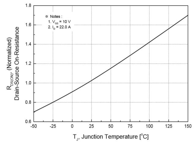
MOSFET RDS(on) is the total resistance of all elements between the drain and source when the device is turned on. RDS(on) has a positive temperature coefficient, meaning it increases as the temperature increases. This is because the mobility of majority-only carriers (holes or electrons) in the MOSFET channel decreases as temperature increases, so does the resistivity. The relationship between the RDS(on) and device junction temperature is not linear. It’s a high order polynomial function of absolute temperature:
RDS(on) (T) = RDS(on) (25C) x (T/300)2.3
RDS(on) is also highly related to the Gate-Source voltage VGS and the drain current ID. Higher VGS can lower the channel resistance, while higher current increases the resistance as the channel is more crowded. As the plot indicates, at a certain VGS, RDS(on) drastically reduces as the device reaches the point where the channel starts to establish and the channel becomes conductive. This VGS is called the threshold, VGS(th). When VGS continuously increases to VGS(sat), RDS(on) becomes nearly constant, which means the device enters the saturation region and the resulted RDS(on) is the lowest. When VGS reaches the maximum allowable value, the gate oxide begins to break down leading to the irreversible damage to the device.


The power dissipation PD of the MOSFET determines the temperature it can reach under certain ambient conditions with or without thermal management. As the device model suggests, the thermal characteristics of a MOSFET consists of the junction temperature TJ, case temperature TC, junction-to-case thermal resistance RθJC, etc.
TJmax = TC + RθJC x PD
ID(TC) =((TJmax – TC)/(RDS(on)(TJmax) x RθJC))0.5

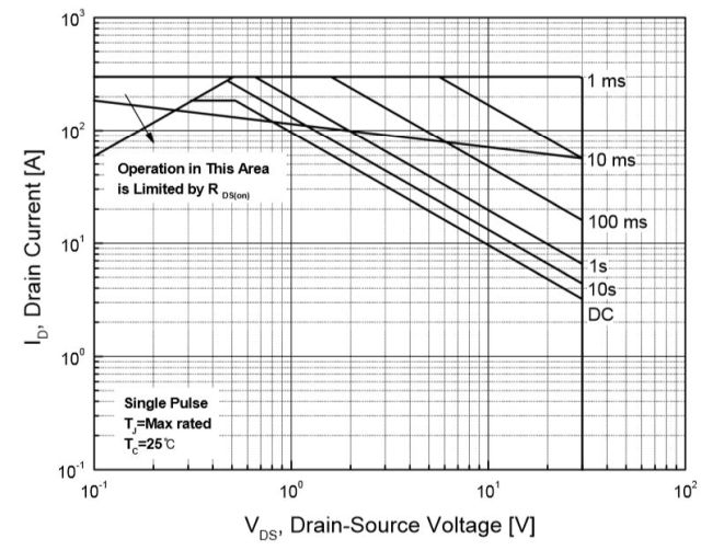
The following plot shows the characteristics of SOA (Safe Operation Areas) of the trench MOSFET. SOA indicates the maximum ratings of VDS (Drain-Source voltage) and ID (Drain current) that ensures safe operations when the device is under forward bias. Therefore, SOA is also denoted as FBSOA (Forward Bias SOA). AS the plot shows, the working conditions under various extremes define the boundaries of the SOA. The right vertical line defines the limit of drain-source voltage of the device, it is called the breakdown voltage. The top horizontal line is the limit of the pulsed drain current IDM. The lines with negative slope between the drain current and breakdown voltage is the pulsed power dissipation, PDM = VDS x ID. The line with negative slope on the left side defines the maximum RDS(on), VDS/ID.