Linear regulator has been widely used by a variety of applications for long time. Before switching mode power supply (SMPS) became popular after 1960s, linear regulator was the basis for the power supply industry. Even though the switching mode power supply represents most used in various applications, linear regulators still find their usage in many applications due to low cost, low noise, simplicity and performance. LM1117 is a popular output voltage adjustable LDO regulator. It provides high precision, current limiting and thermal shutdown. With only two external resistors, the output voltage can be set from 1.25 to 13.8V. Also, it is available in five fixed voltages, 1.8V, 2.5V, 2.85V, 3.3V, and 5V. LM1117 circuit includes a Zener trimmed bandgap reference to assure the output voltage accuracy to within +/- 1%. The following discussion is about LM1117 3.3V version. Unlike the traditional 5V standard that have been widely used in TTL logic, modern High-Speed CMOS (HCMOS) circuits use lower voltage to lower the power consumption. It shows the circuits at 3.3V typically consume 50% or less power than the same circuit at 5V.
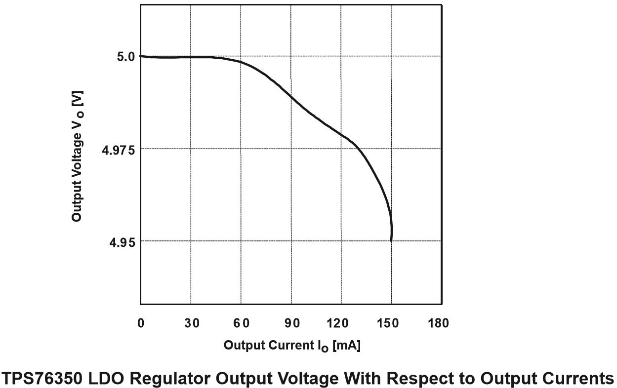
LM1117 is an excellent LDO (Low Dropout) linear regulator. The specs state the maximum dropout is 1.2V at a load current of 800mA. We know the dropout of linear regulator is a function of its load current. We are interested in the calculation of output current to determine the dropout voltage.
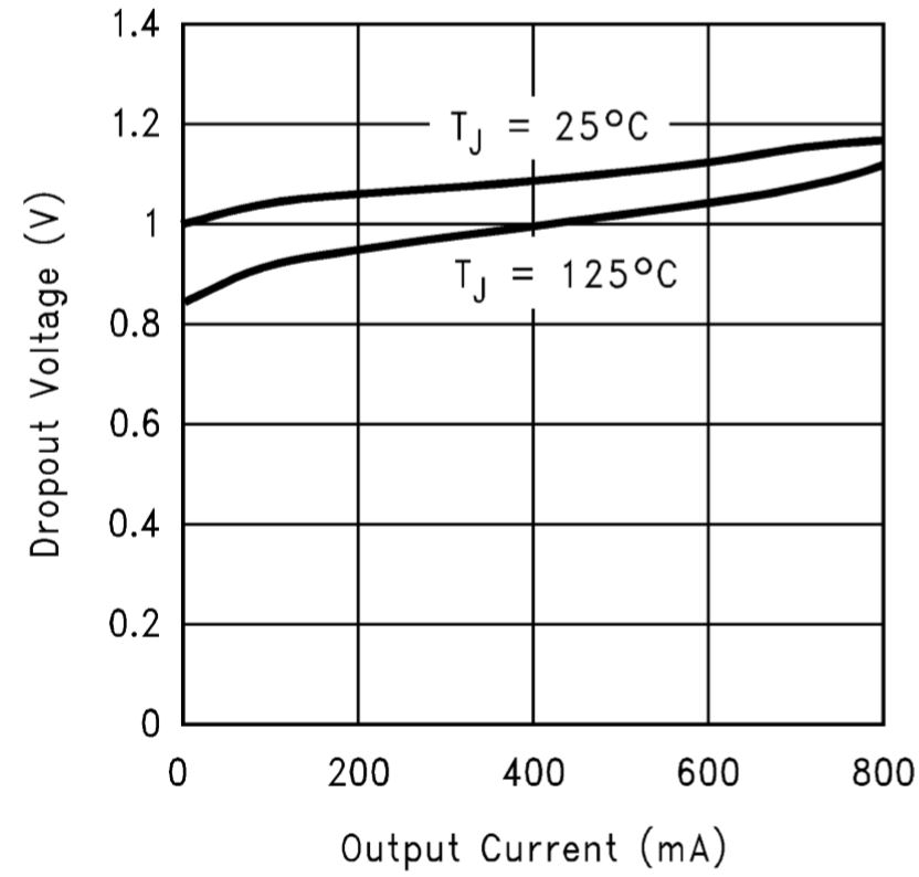
Linear Regulator Dropout voltage (VIN-VOUT)
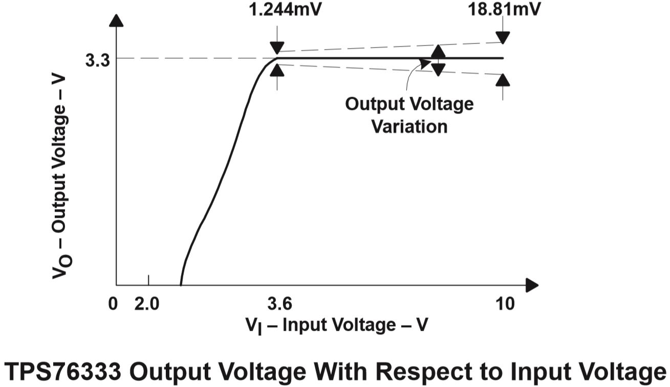
As shown in the above figure, the dropout voltage will vary with output current and temperature. Care should be taken during design to ensure the dropout requirement is met across the entire operating temperature and output current range.
Power Dissipation
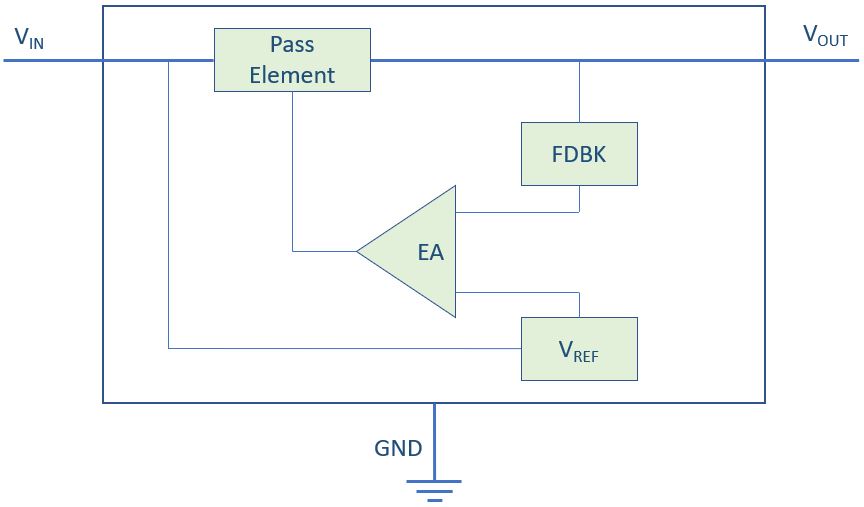
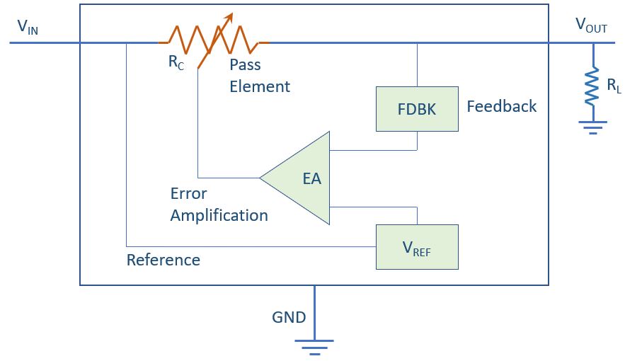
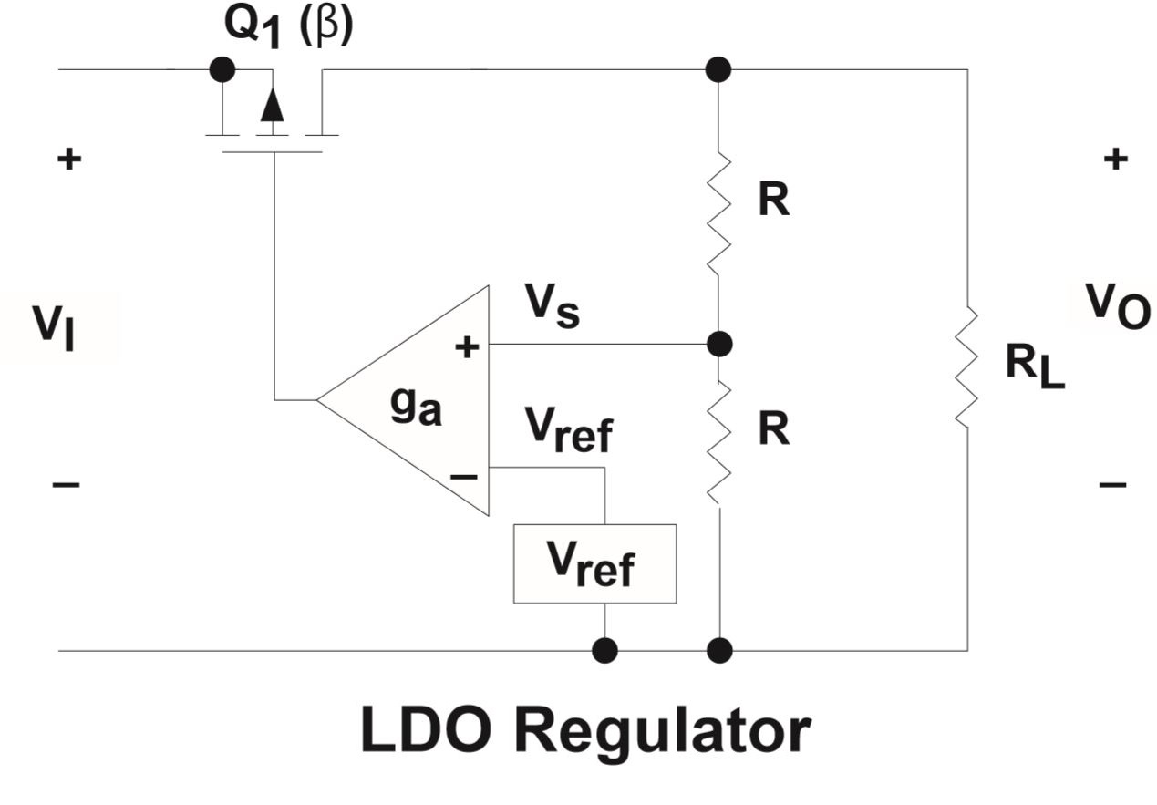
The fundamental function blocks of the linear regulator as shown below. The linear regulator consists of a series pass element that is usually a BJT or MOSFET. The pass element is controlled by an Error Amplifier (EA) that takes an input from the feedback network and another input of the reference voltage (VREF). In the following diagram, the other features are not shown, such as thermal shutdown, overcurrent protection circuit, enable input, error flag output and control voltage feature.
The pass element is installed between VIN and VOUT and the power dissipation of the pass element is the most in the linear regulator. The calculation of power dissipation of the linear regulator is straightforward, the voltage drop across the regulator multiplies the load current. There is also some additional power loss, e.g. power loss due to the biasing current flowing into the ground (thus called ground current). The ground current is usually very small, and it can be ignored because it’s so small that its thermal effect is omitted.
PD = (VIN-VOUT) * IOUT + IGND * VIN
By ignoring the ground current, we have the power dissipation as
PD ≈ (VIN – VOUT) * IOUT
PD: power dissipation in Watts
VIN: Input voltage
VOUT: Output voltage
IOUT: the output current or Load current
IGND: ground current (biasing current)
The voltage drop across the regulator is VLDO = VIN-VOUT.
The pass element of the linear regulator acts as a variable series resistor placed between the input and output and thus causes a voltage drop on the variable resistance. The variable resistance model of the linear voltage regulator is shown below. A control element manipulates how the resistance varies according to the feedback of the output voltage so that the output voltage will remain constant no matter how the input voltage changes. Because of the dropout voltage, the input voltage must be higher than the output voltage. This is called the headroom of the linear regulator.
The controlling resistance RC << RLoad
The input voltage VIN is changing as a function of time while the output voltage VOUT is kept constant. Using Ohm’s Law, we have
VOUT = RLoad/(RLoad+RC) * VIN
In order to get constant VOUT, RC must be
RC = RLoad * (VIN/VOUT – 1) = RLoad * (VIN-VOUT)/VOUT = RLoad * (VLDO/VOUT)
AS we have defined, VLDO = VIN – VOUT
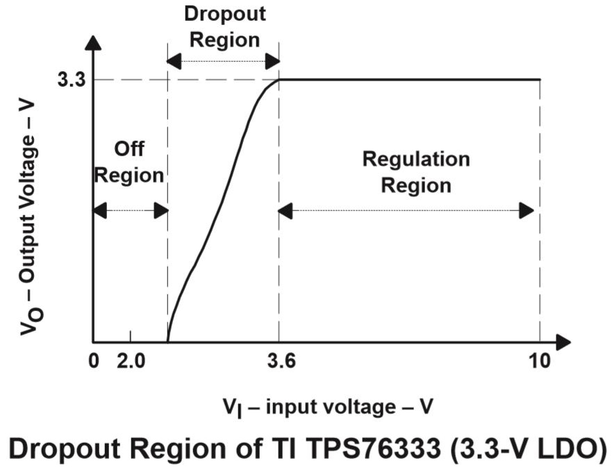
Dropout voltage is the input to output differential voltage at which the circuit stops to regulate against further reductions in input voltage; this point occurs when the input voltage approaches the output voltage. In the dropout region, the pass element is simply a variable resistor and the dropout voltage is the function of its on-resistance RDS(on).
VLDO = IOUT x RDS(on)
Thermal Analysis
Based on the generic model of an LDO regulator, we have the power dissipation PD:
PD = (TJ – TA)/θJA
PD is the power dissipation in watts (W)
TJ is the junction temperature rating (°C)
TA is the ambient temperature (°C)
θJA is the thermal impedance from the junction to ambient (°C/W)
The above equation indicates the thermal performance of the device is dependent on the device material and package, as well as the ambient temperature. The equation can be used to calculate the heat dissipation based on the selected device with specific package under certain ambient temperatures. If we transform the the above equation into the following form, we can use the result for selecting the right device with desirable package.
θJA = (TJ – TA)/PD
Let’s give an example using TI’s 3.3V ultra-low power LDO TPS 76933.
VIN = 5V + 5%
VOut = 3.3V +/- 2%
IOUT = 100 mA
TA = 50C, free air flow
PD,max = (VIN – VOUT) x IOUT = ((VIN x 1.05) – (VOUT X0.98)) x IOUT = (5.25 – 3.234) X 0.1 = 0.2016W
(TJ – TA) = PD x θJA = 0.2016W x 259°C/W = 52.2°C
TJ = 52.2°C + 50°C = 102.2°C
Efficiency
The quiescent current IQ consists of biasing current (such as band-gap reference, sampling resistor, and error amplifier currents) and the gate drive current of the series pass element, which do not contribute to output power. The quiescent current is mostly dependent on the series pass element, topology and ambient temperature, etc.
The quiescent current (or ground current) of an LDO is the combination of the bias current and drive current of the pass element and is normally kept as low as possible.
Additionally, when PMOS or NMOS FETs are used as the pass element, the quiescent current is relatively unaffected by the load current. Since the quiescent current doesn’t pass through to the output, it influences the LDO’s efficiency, which can be calculated by the follow equation:
Efficiency η = IOUT * VOUT/[(IOUT + IQ) * VIN] x 100%
The power dissipation inside the LDO is defined by: IN × (Q + OUT) − OUT × OUT. To optimize the LDO’s efficiency, both quiescent current and the difference between the input and output voltages must be minimized. The difference between the input and output voltages have a direct impact on efficiency and power dissipation, so the lowest dropout voltage is generally preferred. If we ignore the quiescent current, we get the maximum efficiency an LDO regulator can have:
Efficiency η = POUT/(POUT + PLOSS)
= VOUT x IOUT/(VOUT x IOUT + VLDO x IOUT)
= VOUT x IOUT/(VOUT x IOUT + (VIN -VOUT) x IOUT)
= VOUT x IOUT/(VIN x IOUT)
= VOUT/VIN
= (VIN-VLDO)/VIN
= 1 – VLDO/VIN
Even though an LDO cannot deliver high efficiency conversion compared to a switching-mode power supply (SMPS), it is still a necessary voltage regulator for many modern applications. In noise sensitive applications, it is very challenging for an SMPS to achieve the necessary output ripple to meet a tight noise specification. Consequently, it is not uncommon for an LDO to be added as an active filter to the output of an SMPS. This LDO must have high PSRR at the SMPS switching frequency.
LDOs are particularly suited to applications that require an output voltage regulated to slightly below the input voltage. While buck and boost converters have limitations on the maximum/minimum duty cycle, their output voltage will lose regulation with an input voltage that is close to the output voltage.
Example:
A linear LDO regulator has an input voltage range from 3.6V to 4.5V, and the output current range is from 80mA to 100mA. The maximum quiescent current is 17uA, the minimum efficiency is
Efficiency η = 100mA x 3.3V/[(100mA+17uA) x 4.5V] x 100 = 73.3%
Line regulation
Line regulation is a steady state specification and a measure of the circuit’s ability to maintain the specified output voltage with varying input voltage.
Line regulation = ΔVOUT/ΔVIN = (VOUT@VIN_Max – VOUT@VIN_Min)/(VIN_max – VIN_min)
Increasing the open loop gain improves the line regulation.
Since line regulation is also dependent on the performance of the pass element and closed-loop DC gain, dropout operation is often not included when considering line regulation. Hence, the minimum input voltage for line regulation must be higher than the dropout voltage.
Load regulation
The load regulation is a measure of the circuit’s ability to maintain the specified output voltage under varying load conditions.
Load regulation = ΔVOUT/ΔIOUT = (VOUT@no_load – VOUT@full_load)/(0 – IOUT@full_load)
The worst case of the output voltage variations occurs as the load current transitions from zero to its maximum rated value or vice versa. As the line regulation, increasing the open loop gain improves the load regulation.
Load regulation indicates the performance of the pass element and the closed-loop DC gain of the regulator. The higher the closed-loop DC gain, the better the load regulation.
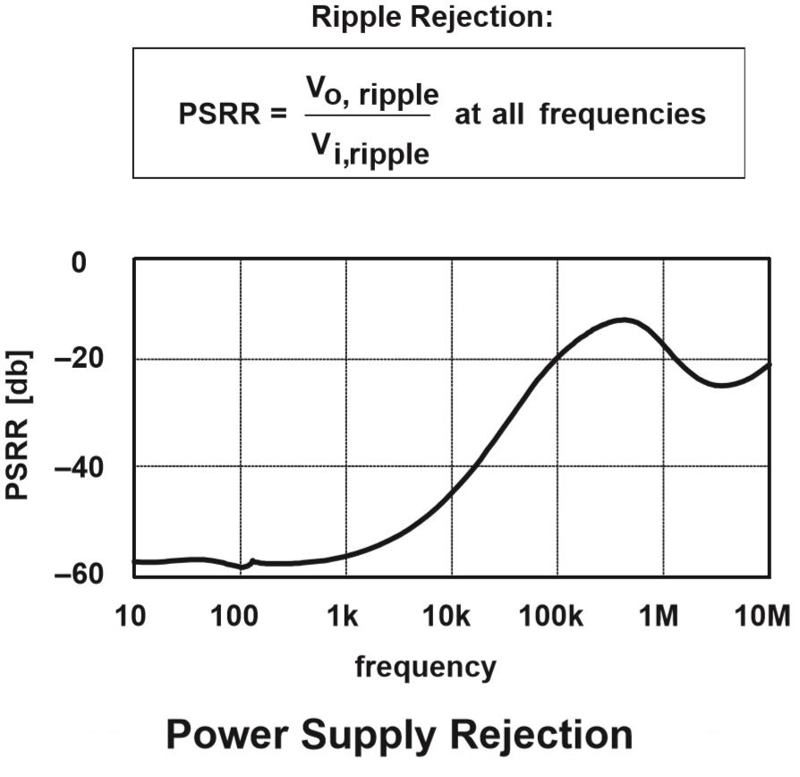
Power Supply Rejection Ratio (PSRR)
Power Supply Rejection Ratio (PSRR) is known as ripple rejection and is used to measure the LDO’s ability to prevent the regulated output voltage fluctuation caused by input voltage variations. The same relation for line regulation applies to PSRR except that the whole frequency spectrum is considered. PSRR is defined as the ratio of output noise to input noise at different frequencies. It represents the capability of the regulator to suppress noise from the input to the output. PSRR is very important for RF sensitive applications. We can use either a digital oscilloscope or a network analyzer with two high impedance probes. The following figure shows the input and output AC signal waveforms (ripples) of TI’s TPS78101.

From the above waveforms, we have the following results:
Ripple_Input = 984 mV
Ripple_Output = 194 mV
PSRR = 20 log(Ripple_Input/Ripple_Output) = 20 log(984/194) = 14.1dB
Accuracy
The overall accuracy considers the effects of line regulation (ΔVLR), load regulation (ΔVLDR), reference voltage drift (ΔVOUT, ref), error amplifier voltage drift (ΔVOUT,ea), external voltage divider feedback resistor tolerance (ΔVOUT,res) and temperature coefficient (ΔVTC).
Accuracy ≈ [(|ΔVLR| + |ΔVLDR|+SQRT(ΔVOUT, ref ^2 + ΔVOUT,ea ^2 + ΔVOUT,res ^2 + ΔVTC ^2))/VOUT] x 100
Example:
Calculate the overall accuracy of the 3.3V LDO linear regulator sown in the above circuit over the temperature range from 0° to 125°C. The temperature coefficient is 100 ppm/°C, feedback resistor tolerance is 0.25%, the output voltage change resulting from load regulation and line regulation are ±5mV and ±10mV respectively. The accuracy of the reference voltage is 1%.
The output voltage is determined by:
VOUT = (R +R) x Vref/R = 2Vref
Or Vref = 0.5 VOUT
ΔVOUT, ref =[ (R + R)/R] x (Vref x 1%) = 2 x (Vref x 1%) = 33 mV
ΔVOUT,res = (0.25% + 0.25%) x Vref = 0.005 x (3.3/2) = 8.25 mV
ΔVTC = Temperature Coefficient x (Tmax – Tmin) x VOUT = 100 x 10-6 x (125 – 0) x 3.3 = 41.25 mV
Accuracy ≈ [(|ΔVLR| + |ΔVLDR|+SQRT(ΔVOUT, ref ^2 + ΔVOUT,ea ^2 + ΔVOUT,res ^2 + ΔVTC ^2))/VOUT] x 100
= [(10 mV + 5 mV + SQRT(33 mV^2 + 0 + 8.25 mV^2 + 41.25 mV^2))/3300 mV] x 100%
≈ 2.075%
Design considerations for typical applications of LM1117 LDO regulator
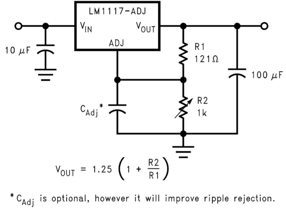
One of the advantages of using LM1117 is the small count of components LM1117 requires. As shown in the above circuit, it requires two resistors to form a voltage divider for output feedback. A capacitor on the output is need for load regulation. The capacitor on the output pin is important to maintain the regulator stability. The capacitance of the output capacitor must meet the requirements for both the minimum capacitance and equivalent series resistance (ESR). LM requires the minimum output capacitance be 10 µF if a tantalum capacitor is to be used. Increasing the output capacitance starting from 10 µF will improve the loop stability and transient response of the regulator. The ESR of the output capacitor should be in the range from 0.3 Ω to 22 Ω. In case the bypass capacitor on the adjust pin is used, a large output capacitor (e.g. 22µF tantalum) must be used. Also, a capacitor on the input pin is also recommended as the input bypass capacitor.
As shown in the above circuit, a bypass capacitor between the adjust pin and ground can be used to bypass the adjustment to improve ripple rejection performance. When the output voltage is increases, the ripples are amplified. The adjust pin bypass capacitor is used to bypass the ripples to ground before they are amplified. Based on the above application circuit, at any ripple frequency, the impedance of the CADJ should be less than R1 to prevent the ripple from being amplified:
XCADJ = 1/(2π x fRipple x CADJ) < R1
R1 is normally in the range of 100-200 Ω. If we select R1 to be 150 Ω, and the ripple frequency fRipple = 150 Hz, the CADJ should be > 7.1 µF.