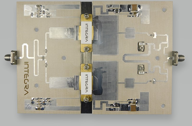
El Segundo, CA based Integra Technologies Inc (ITI) announced an RF power amplifier module/pallet, IGNP1011L2400 that was expected to resolve the challenge of SWaP-C (size, weight, power and cost) in high performance L-Band avionics systems. Integra is known as a manufacturer of high-power RF and microwave transistors and power amplifier modules (known as high power amplifiers or HPAs). The new RF power amplifier IGNP1011L2400 is an RF high power amplifier manufactured with Gallium Nitride on Silicon Carbide (GaN-on-SiC) technology. The device is specifically designed for IFF/SSR (Identification Friend or Foe/Secondary Surveillance Radar) applications operating under either the ELM (Extended Length Message) Mode S (48-pulse burst with each pulse being 32us ON and 18us OFF, 6.4% long term duty cycle) or Standard Mode S (128us 2% duty cycle) pulse conditions.
The new GaN-on-SiC device supplies a minimum of 2200W of peak output power, with typically greater than 16dB of gain and 57% efficiency and operates from a 50V supply voltage. The RF power amplifier module/pallet is matched to 50 ohms at both input and output and is suitable for both 1030MHz and 1090MHz frequencies.
GaN-on SiC HEMT, namely the Gallium Nitride on Silicon Carbide High Electron Mobility Power Transistor has been a matured technology since last few years. They have been used on various applications, such as pulsed radars, counter-IED jammers to CATV modules and fourth-generation infrastructure base stations. GaN HEMT devices have demonstrated high power densities with high breakdown voltages along with the low on-resistance and opened the possibilities for highly efficient power amplifiers (PAs).
Wide-bandgap GaN-on-SiC HEMT’s high breakdown voltages allow large drain voltages to be used leading to high output impedance per unit RF power output, which results in easy impedance matching circuitry. Their high sheet charge leads to high current density and reduced die area for equivalent output power density. These devices use high mobility carriers that contribute to high saturation current densities as well as watts per unit gate periphery. The overall effect of the high saturation velocity is the low capacitances per watt of output power. The unique characteristics of low output capacitance and drain-to-source resistance per watt make GaN HMETs good for switch -mode amplifiers.
Historically, Silicon LDMOS became the main technology for communications and base stations in mid 1990s and soon widely accepted for L-Band avionic and radar applications due to the low cost of manufacturing compared with traditional bipolar RF power transistors. GaN HEMT technology became intensively studied in the decade from late 1990s to early 2000s starting with growing high-quality 4H-SiC substrates that are semi-insulating and superior for high power performance and thermal management. Compared with Silicon LDMOS, GaN HEMT devices have a lower on-resistance for the same output power to maintain a higher efficiency.