Samsung’s 3D V-NAND flash and Crossbar’s RRAM memory
As the market of portable devices, such as USB drives, digital cameras, Smartphone and ultrabook PC's, continues increasing, Non-volatile memories use by these devices, which have low power consumption and low cost have gained their market.
According to IHS iSuppli, the global NAND flash memory market is reaching $30.8 Billion in revenues by 2016, an large increase from about $23.6 Billion in 2013.
It has been shown that power consumption in data storage and information retention in memory systems account for a considerable portion of the oeverall system power consumtion. Compared to other popular non-volatile technologies, such as FerAM (Ferroelectric RAM), MRAM (Magnetic RAM) and PCM (Phase Channge Memory), NAND flash memory is presently the most attractive solution to the difficulties encountered when scaling the device sizes to achieve high device capacity, low energy consumption, low fabrication cost, high performance, etc.
It has been found that the flash memory scaling is faster than the famous Moore's Law that states the integration density increases by 100% every 1.5 years. Therefore it is expected that scaling of flash memory will encounter many difficulties, such as further increased parasitic floating -gate interferences and decreased gate-coupling ratio. The floating gate technique has been applied to solve these issues.
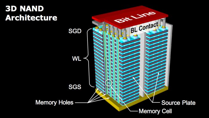
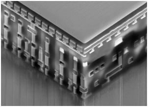
The start of mass production of 3D NAND Flash memory chips announced August 6, 2013 by Samsung indicates the flash scaling has gone to 3D extreme from the traditional planar architectures. After 10 years of R&D by Samsung, the first 3D NAND flash memory (V-NAND) chip will be 128 GB in a single chip fabricated vertically in structure. The V-NAND flash memory employs Samsung's CTF (Charge Trap Flash) technology. Contrast to the floating gate technology, the CTF based NAND flash structure, places the charge in a SiN (Silicon Nitride) dielectric layer to prevent the interference between neighboring cells due to further scaling. Therefore by applying the CTF 3D architecture, we can improve the reliability while further scaling the device vertically. It is expected to have as many as 24 cell layers vertically by using special etching technology and interconnect process. According to Samsung, the V-NAND flash memory provides 2X performance and minimum 2X/maximum 10X reliability compared to the standard 10nm NAND flash memory.
As the 3D V-NAND flash memory promises to provide incomparable advantages over the traditional memory technologies, we naturally ask the question, “is the 3D technology the only good solutions to our increasing memory needs?"
Contrast to Samsung’s 3D V-NAND flash that is charge-based device, RRAM (Resistive Random Access Memory) is resistive switching based device, a technology is based on different physical phenomenon and is widely hailed as the “most likely to succeed” in the race to develop a new, more scalable, high capacity, high performance and reliable memory, according to the start-up Crossbar Inc.
The typical non-volatile RRAM cell has a three layer structure with a switching medium sandwiched by the top and bottom metallic electrodes. The memory cell’s switching effect is realized by altering the resistance of the middle layer that is a special type of dielectric material. There are several types of inorganic or organic materials that demonstrate resistive switching effects under certain thermal or electric field conditions, which can cause migration of ions into the switching medium and thus results change of resistance of the medium layer.
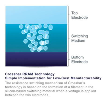
(Source: Crossbar Inc.)
Even though it will take another 1 to 2 years to have the first prototype RRAM memory chips available according to several companies that are developing RRAM flash devices, many advantages of RRAM memory over NAND flash memory have been discussed.
Crossbar Inc has proven the RRAM could be manufactured with the standard CMOS technology, which means they can apply 3D stacking technology to manufacturing 3D RRAM devices similar to the Samsung V-NAND flash memory. The following figure from Crossbar Inc. illustrates the potential advantages of RRAM over the standard NAND flash memory.
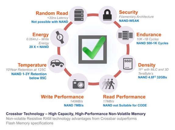
In summary:
- Low temperature cell: enables the integration of multiple memory array layers on top of the CMOS controller and provides potential 1TB storage capacity.
- Provides 1/10th of programming current for low-power applications, 2 to 4 times more data (MLC) and 1 to 3 more stacking layers for greater density.
- Cell switching based on field dependent switching: leads to no read- or program-disturb below the critical field.
- No joule heating: eliminates cross talk between the cells during the switching event and allows for larger arrays and higher density.
- No need for high voltage devices for multiple program/erase cycles: allows smaller die sizes and cheaper process technology.
- Mitigated potential memory loss from the program-state and the erase-state due to our field dependent switching phenomena.
- Large on/off ratio: improves as cell size shrinks.
- Tight distribution across the wafer: provides good margin for product design.
- No diffusion of metal during normal backend thermal processing: enables easily port to backend CMOS processing.
[get_social_code]