The first single-atom-thick carbon-based material, graphene was discovered in 2003 and it has driven intensive studies in other types of 2-D materials.
The most distinct characteristics of these materials is that they can be stacked together like Lego bricks. This characteristic has been utilized to create devices with different functions, including operating as semiconductors. The 2-D (2 dimensional) nature of these materials have opened the door to create ultra-thin, flexible, transparent and wearable electronic devices.
The difficulty of making 2-D flakes from bulk crystal material has prohibited it from commercial production of electronics with the current process and technology, which splits each individual flake from a bulk crystal by stamping the crystal onto a sticky tape. This process has been shown unreliable and with low productivity.
Now researchers in the Department of Mechanical Engineering at MIT have developed a technique to harvest 2-inch diameter wafers of 2-D material within just a few minutes. They can then be stacked together to form an electronic device within an hour.
The technique, which they describe in a paper published in the journal Science, could open up the possibility of commercializing electronic devices based on a variety of 2-D materials, according to Jeehwan Kim, an associate professor in the Department of Mechanical Engineering, who led the research. The authors of this paper included students and postdocs from within Kim’s group, as well as collaborators at Georgia Tech, the University of Texas, Yonsei University in South Korea, and the University of Virginia. Sang-Hoon Bae, Jaewoo Shim, Wei Kong, and Doyoon Lee in Kim’s research group equally contributed to this work.
The principle of the process is that materials with layered structure have much stronger adhesion force to nickel than to sapphire. The team first grew a thick stack of 2-D material on top of a sapphire wafer. They then applied a 600-nanometer-thick nickel film to the top of the stack. Finally, a liftoff process separates the stack of grown 2-D material from the sapphire wafer. Also, the adhesion force between the nickel layer and the first layers of the stack is greater than the force between the following individual layers. So after the team applied another layer of nickel to the bottom of the stack, the team could eventually separate the stack of 2-D materials layer by layer with a thickness of single atom. That is because peeling off the first nickel film generates cracks in the material that propagate right through to the bottom of the stack, Kim says. Once the first monolayer collected by the nickel film has been transferred to a substrate, the process can be repeated for each layer.
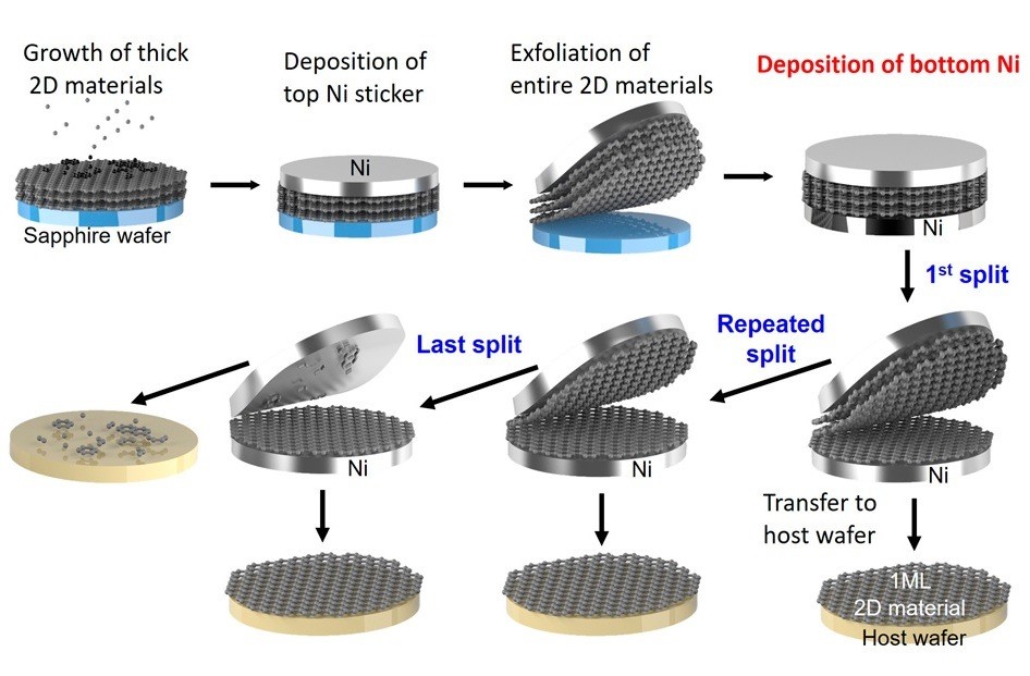

“We use very simple mechanics, and by using this controlled crack propagation concept we are able to isolate monolayer 2-D material at the wafer scale,” he says. The universal technique can be used with a range of different 2-D materials, including hexagonal boron nitride, tungsten disulfide, and molybdenum disulfide. In this way it can be used to produce different types of monolayer 2-D materials, such as semiconductors, metals, and insulators, which can then be stacked together to form the 2-D heterostructures needed for an electronic device.
“If you fabricate electronic and photonic devices using 2-D materials, the devices will be just a few monolayers thick,” Kim says. “They will be extremely flexible, and can be stamped on to anything,” he says. The process is fast and low-cost, making it suitable for commercial operations, he adds. The researchers have also demonstrated the technique by successfully fabricating arrays of field-effect transistors at the wafer scale, with a thickness of just a few atoms.
“The work has a lot of potential to bring 2-D materials and their heterostructures towards real-world applications,” says Philip Kim, a professor of physics at Harvard University, who was not involved in the research. The researchers are now planning to apply the technique to develop a range of electronic devices, including a nonvolatile memory array and flexible devices that can be worn on the skin. They are also interested in applying the technique to develop devices for use in the “internet of things,” Kim says. “All you need to do is grow these thick 2-D materials, then isolate them in monolayers and stack them up. So it is extremely cheap — much cheaper than the existing semiconductor process. This means it will bring laboratory-level 2-D materials into manufacturing for commercialization,” Kim says. “That makes it perfect for IoT networks, because if you were to use conventional semiconductors for the sensing systems it would be expensive.”
Reference
- Jaewoo Shim, Sang-Hoon Bae, Wei Kong, Doyoon Lee, Kuan Qiao, Daniel Nezich, Yong Ju Park, Ruike Zhao, Suresh Sundaram, Xin Li, Hanwool Yeon, Chanyeol Choi, Hyun Kum, Ruoyu Yue, Guanyu Zhou, Yunbo Ou, Kyusang Lee, Jagadeesh Moodera, Xuanhe Zhao, Jong-Hyun Ahn, Christopher Hinkle, Abdallah Ougazzaden, Jeehwan Kim, “Controlled crack propagation for atomic precision handling of wafer-scale two-dimensional materials”, Science 11 Oct 2018: eaat8126, DOI: 10.1126/science.aat8126
- http://news.mit.edu/2018/researchers-quickly-harvest-single-atom-materials-1011