Op Amps (Operational Amplifiers) have been widely used in many applications since its solid-state monolithic version was invented in 1963. The typical applications of op amps include sensor signal processing, voltage followers, comparators, filters, differentiators, integrators, phase shifters, amplifiers, voltage-to-current converters, etc. Even though op amps have great success in general purpose applications, their usage in areas such as sensors requiring high accuracy face challenges due to some intrinsic limitations, such as input offset voltage and input offset voltage drift.
Sensors have been used everywhere in our modern life, from consumer, automotive, industrial to medical applications. They have been facing worse environmental challenges than ever, such as EMI (Electromagnetic Interference), ESD (Electrostatic Discharge) spikes, power supply ripples, ground loop errors. On the other hand, in special applications, like wireless sensor network, portable devices, wearables, IoT (Internet of Things) and other battery-powered applications, the signals become small and the rail-to-rail swing is marginal, at the same time, low-power consumption is a pursuit for all applications. All these challenges are ultimately focused on the op amp sitting at the center of the analog portion of the ADC (Analog to Digital Converter).
When we learned the theories of op amps, they were treated as ideal op amps in textbooks. We established that when the input voltage applied to the input pins was zero volt, the output of the op amp should be nothing but zero volt. In real world we all find that is not true. If we get zero volt on the output pins, we must see non-zero input across the input pins, which we call it Input Offset Voltage and is referred to as VOS. This intrinsic differential voltage stems from the inherent mismatch of the transistors and supporting components in the input section of the op amp during wafer and die fabrication processes. Furthermore, during the process of device packaging, stresses induced by metal-semiconductor bonding can be another contributor to the undesirable mismatch. The combining effect of all factors creates a mismatch of the bias currents flowing through the input circuit of the op amp, resulting in a voltage differential at the input pins.
In the applications, the differential input voltage VOS is added to the signal’s output voltage by multiplying the closed-loop gain of the op amp, which adds a significant error factor to the output. In the past time, many approaches have been taken to compensate/reduce the VOS effect, such as improved technology on the silicon material processing, better bonding materials, matching components and device trimming procedures. For better performance, zero-drift op amps have been produced by many manufacturers. A zero-drift operational amplifier is an op amp that has reduced input offset voltage and input offset voltage drift with respect to temperature and time. According to the reasons we mentioned before, it is very important to use a zero-drift operation amplifier in applications that require high-accuracy signal amplification.
Zero-drift op amps contain circuitry that automatically corrects the input offset voltage. This circuitry is categorized as one of the following three types that are referred to as three auto-drift architectures:
- Auto zero amplifier
- Chopper amplifier
- Combined auto-zero and chopper amplifier
Zero-drift op amps have helped users to achieve the general design specifications like:
- Temperature offset drift
- Input offset voltage
- 1/f noise
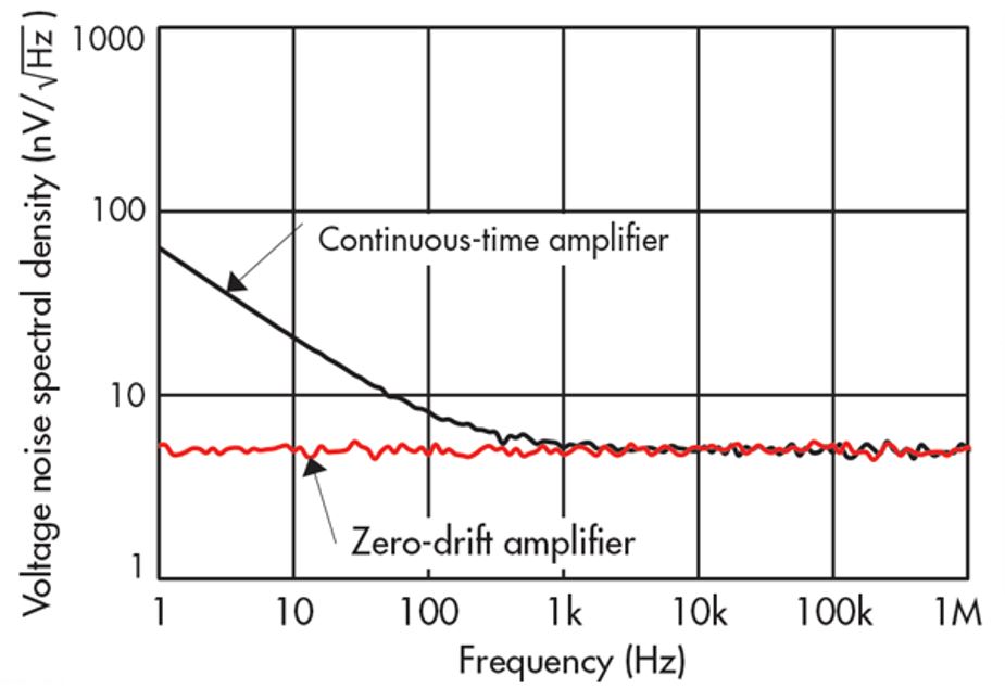
One of the most important sources of ADC (Analog-to-Digital Converter) error is noise. Modern ADC is usually integrated with signal processing circuitry that should filter out completely the noise component in the signal, which is an impossible task. The remaining noise still goes through the conditioning circuitry that tries to amplify not only the signal but also the left-over noise at the same time with the same gain. Therefore, it leads to design low-noise analog front-end to get the optimal SNR (or S/N, Signal to Noise Ratio) for applications requiring high precision. The noise in ADC exists in two types, 1/f noise (also called pink noise or flicker noise) and white noise. It is more prominent in the low-frequency domain (< 100 Hz) due to the irregularities in the conduction path and the bias currents within the input transistors. Compared to BJT (Bipolar Junction Transistor) that were preferred in designing traditional low-noise analog input stage circuit, CMOS input stage design tends to have the noise with a higher amplitude and a higher corner frequency (this the frequency where the pink noise density equals the white noise) than BJT devices. At higher frequencies, 1/f noise is less significant because the white noise from other sources becomes dominant and this is exactly why it is called 1/f noise. This low-frequency 1/f noise can cause big trouble if the input signal is nearly DC like, which is typically observed in the output signals of strain gauges, pressure sensors, thermocouples or any slow-changing signals. The following figure shows how zero-drift topology practically eliminates 1/f noise (Texas Instruments).
Zero-drift amplifiers provide many benefits to designers, as temperature drift and 1/f noise, always nuisances in the system, are otherwise very difficult to eliminate. In addition, zero-drift amplifiers have higher open-loop gain, power-supply rejection, and common-mode rejection as compared to standard amplifiers; and their overall output error is less than that obtained by a standard precision amplifier in the same configuration.
On Semiconductor’s NCS333A is a low-power zero-drift op amp features an offset voltage as low as 10 µV over the 1.8V to 5.5V supply voltage range. NCS333A use a chopper-stabilized zero-drift architecture, which helps reduce offset voltage drift over temperature and time.
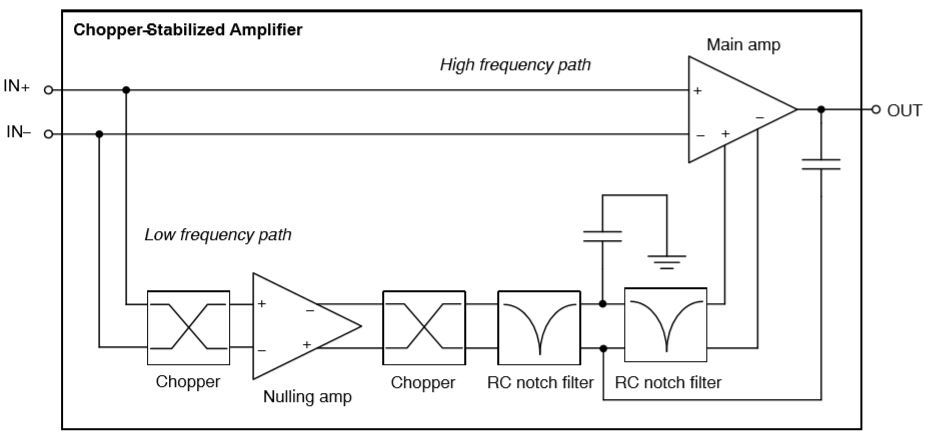
The above Chopper-Stabilized Architecture contains two signal paths. The upper signal path is the feed-forward path that works at higher frequency that extends the gain bandwidth up to 350 kHz. This high frequency feed-forward path retains the high frequency components of the signal and it also improves the closed-loop gain at low frequencies. This offers advantages for low-side current sensing and sensor interface applications where the signal has mainly low frequencies and low differential voltages. The lower path is the feedback path used for sampling the input offset voltage and the feedback is used for correcting the offset at the output. The frequency used for offset correction is 125 kHz. The Chopper-Stabilized architecture is optimized for the best performance up to the Nyquist frequency, which is 62.5 kHz, or 1/2 of the offset correction frequency.
Features:
- Gain – Bandwidth Product (GBWP): 350 kHz
- Low Supply Current: 17 µA (@ 3.3V)
- Low Offset Voltage (VOS): 10 µV
- Low Offset Drift: 0.07 µV/°C max
- Wide Supply Range: 1.8 V to 5.5 V
- Wide Temperature Range: -40 °C to +125 °C
- Rail-to-Rail Input and Output
Applications:
- Automotive
- Battery Powered/Portable applications
- Sensor Signal Conditioning
- Low Voltage Current Sensing
- Filter Circuits
- Bridge Circuits
- Medical Instrumentation
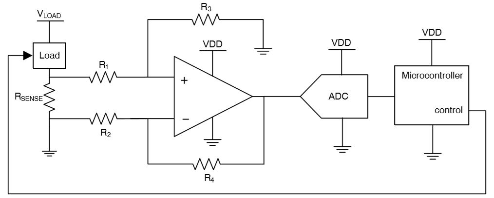
On Semiconductor Zero-Drift Op Amp NCS333A Typical Application of Low-Side Current Sensing Circuit (Source: On Semiconductor)