In portable electronics, automotive system and wireless devices, which use batteries for power, power reliability and battery life are especially important to meet the requirements for performance and added functionalities. At the same time, reduction of cost is another important factor in design considerations. To achieve these goals, we must use advanced PMIC (Power Management IC) to efficiently control every aspect of the power systems from battery charging to battery management as well as various power protections including overvoltage, overcurrent, reverse polarity, load balancing and mode transitioning, etc. Typically, new PMICs have integrated load switches for power output control. The use of PMICs simplifies the designs and reduces cost. On the other side, many portable and miniature applications may not need to use an PMIC to ensure the high performances due to the added complexity, cost of BOM and waste of PMIC resources. In such cases, we can design highly efficient load switches that are directly controlled by the MCUs to control the power output, battery charging and power mode transitioning. Typical load switches are made of MOSFETs, N-Channel or P-Channel due to low drain-source on-resistance. After the low VCE(sat) BJTs were introduced, we have a new option for designing high-efficiency load switches. Even though BJTs have the disadvantages of current-based control, compared to its MOSFET counterpart, BJTs offer many advantages, such as high ESD (Electrostatic Discharge) robustness and low Temperature coefficient for key parameters like VBE and RCE(sat). For example, the Base-Emitter Voltage VBE of BJT has a temperature coefficient of about 2mV/K compared to the Gate-Source Threshold voltage of MOSFET that has a temperature factor of about 4mV/K to 6mV/K. The BJT’s Collector-Emitter saturation resistance RCE(sat) decreases with about 0.4%/K over temperature, whereas the Drain-Source On-Resistance RDS(on) of a MOSFET increases with a factor of 0.6%/K over temperature. Using BJTs can potentially reduce part count in some applications because of removing charge pump components. Also, BJTs naturally block reverse current, which eliminates the need of the blocking diode.
Like MOSFET switches, the loss of power supply on the switching BJT is the product of collector current and the residual voltage measured between the collector and the emitter in the saturation condition as shown by the following equation:
PD = VCE(sat) x IC
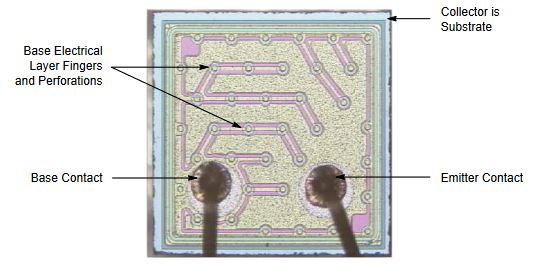
The load current determines the collector current in the application. The only way to reduce the power dissipation is to reduce the VCE(sat). This is the drive for developing the family of transistors called low VCE(sat) BJTs. Based on a technology called “Perforated Emitter”, the die layout design of the low VCE(sat) BJT features a mesh structure that evenly separates the transistor into many cell structures that allow evenly distributed current flow with great efficiency.
The latest low VCE(sat) BJTs provide comparable saturation on-resistance to that of a MOSFET along with many advantages, such as ESD robustness and low temperature coefficient. Using a low VCE(sat) BJT in certain applications will provide better results. The low VCE(sat) BJTs can see applications not only in portable electronics, mobile devices and wireless systems, but also automotive products, such as dash board back lighting, air bag deployment, power protection, LDO regulators, and MOSFET pre-drivers. To assist rapid design, we give the following examples of typical application circuits of low VCE(sat) BJTs.
Load switches
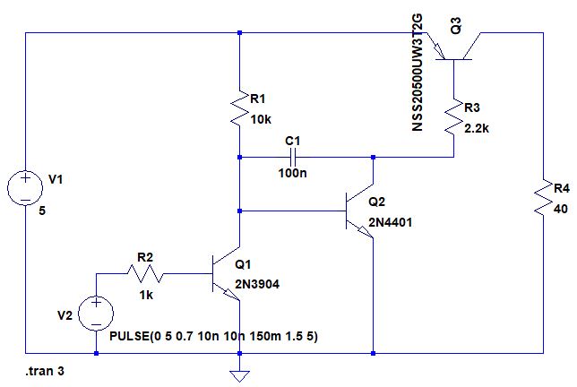
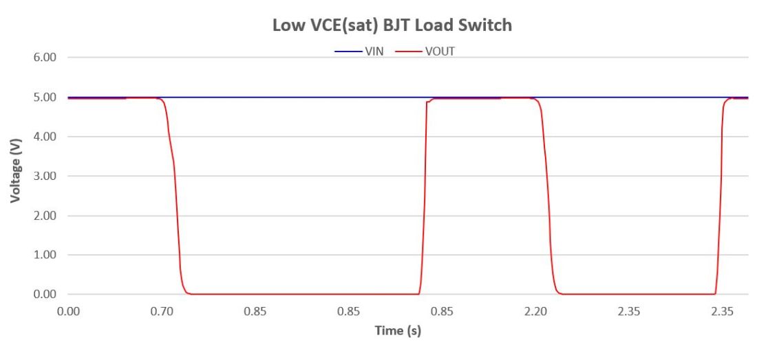
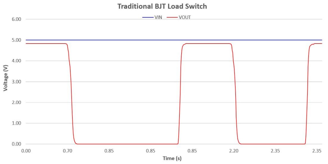
Since the BJT has very low VCE(sat), it is ideal to make a power switch in applications that only require to switch the device ON or OFF, such as seat heaters in cars and dashboard LCD backlight. The following circuit shows the use of On Semiconductor’s low VCE(sat) BJT NSS20500UW3 in a load switch. We use the low VCE(sat) BJT Q3 NSS20500UW3 as the pass element and use the standard NPN BJTs Q1 and Q2 to control the pass element. The output of the low VCE(sat) BJT Q3 is shown below. The source voltage is 5V and the output voltage on the load is nearly 4.958V that is much higher than 4.8V out of a standard PNP BJT. Assuming the load current is 125 mA, we can reduce the power dissipation by the switch by about 20 mW when a low VCE(sat) transistor is used. With the low VCE(sat) BJT, power loss is further reduced on the base bias resistor due to significant reductions in base drive current.
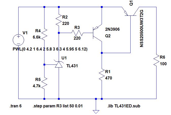
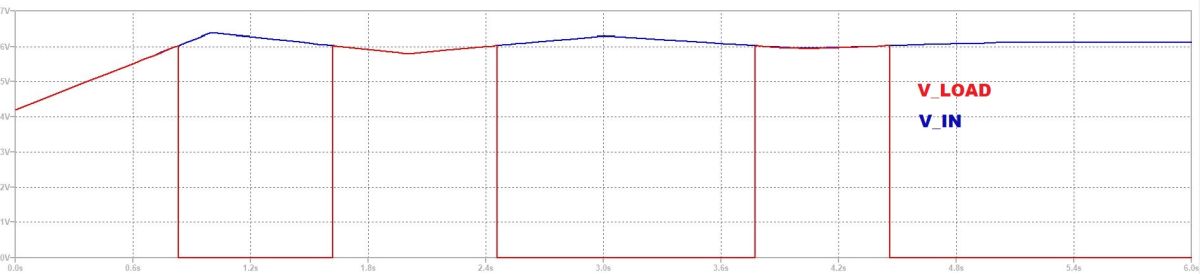
Over voltage protection with Zener and TL431
We can use low VCE(sat) BJT to protect load circuitry against overvoltage conditions. The tripping point at about 6V is set by the voltage divider formed by R4 and R5 in the schematic shown below. The voltage resulted is the reference voltage of the TL431 and it is compared to the internal reference that is 2.495V. When it is larger than the internal reference of 2.5V, TL431 allows current to flow and Q2 2N3906 turns on to force Q1 NSS20500UW3 off. Therefore the output voltage is cut off on the load. When the reference voltage is below the virtual internal reference of 2.495V, little current is allowed to flow from the cathode to the anode of TL431, thus Q2 2N3906 is cut off. Since T2 is cut off, the low VCE(sat) Q1 NSS20500UW3 turns on via the base resistor R1 to pass the input voltage to the load R6 with a loss of VCE(sat) = VIN – VOUT. Therefore a low VCE(sat) BJT is preferred in this application to provide higher efficiency and lower power dissipation on the pass transistor.
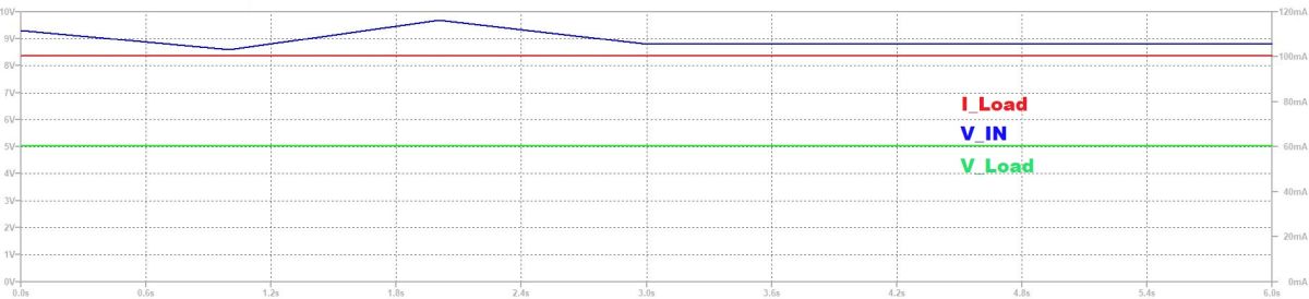
Voltage Stabilizer – Series Pass Regulator
Voltage fluctuation affects performance or even damage the load. Voltage stabilizer or automatic voltage regulator can provide constant voltage to the load even with fluctuating input voltage. Voltage stabilizers can help maintain high performance and protect the device it supplies power. They are especially important for precision instruments, reference voltage sources and healthcare devices. In a DC voltage stabilizer, at a preset output current, there is always a reduction of the voltage on the load caused by the pass element, which is called dropout voltage. The dropout voltage determines the minimum headroom required to maintain the nominal output voltage for desirable line regulation with varying input voltage. The lower the dropout voltage, the higher efficiency the regulator can achieve. Due to the low saturation collector-emitter voltage, the low VCE(sat) BJT is an excellent option as voltage stabilizer. If we use a general purpose BJT as a voltage stabilizer, the dropout voltage would be more than 0.6V or more. In the following circuit of a voltage stabilizer, we juse a TL431 shunt regulator as the voltage reference set by the voltage divider.
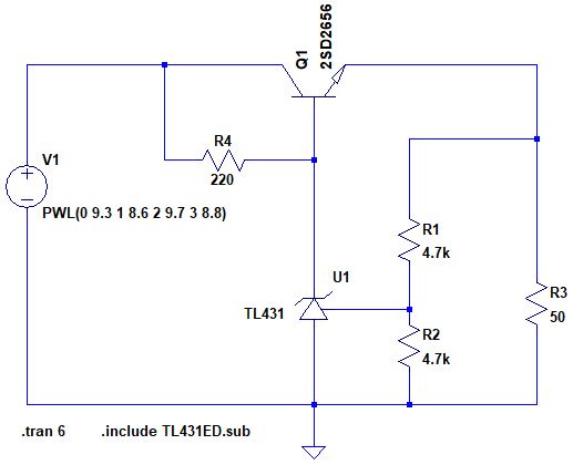
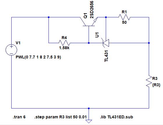
Constant Current Source – Supply Current Limiter
We can use a low VCE(sat) BJT series pass transistor and a shunt regulator TL431 to create a constant current source circuit thatwe can widely use for many applications, such as LED driver, constant current source and short circuit protector or current limiter. The circuit shown is the application of circuit limiter. From the below simulation results, we see the load current changes from 51.69 mA to 53.23 mA when the load resistance changes from 50 ohms to 0.01 ohms. In this example, using a low VCE(sat) transistor offers many advantages, such as low dropout, high efficiency, wide range of input voltage. Size the current sense resistor R1 so that we can determiine the value of the output current for the desired application.